
- Products & Capabilities

- About
- Resources
Fine‑Pitch BGA Design: How Via‑in‑Pad Microvias Optimize Density and Performance


Learn how VIPPO via-in-pad microvias boost routing density, signal integrity & reliability for fine-pitch BGA HDI PCB designs.
Modern electronic devices across consumer, automotive, medical and industrial sectors continuously pursue ultra-compact form factors, faster data transmission speeds, and long-term operational reliability, making fine-pitch Ball Grid Array (BGA) packaging the primary choice for modern high-pin-count integrated circuits. Nevertheless, conventional dog-bone BGA fanout design, which relies on peripheral traces and independent outer-layer vias, faces inherent limitations including wasted routing space, excessive PCB layer stacking, and degraded high-speed signal integrity. As a mature and widely adopted High-Density Interconnect (HDI) manufacturing technology, via-in-pad (VIP) microvia combined with VIPPO (Via-in-Pad Plated-Over) processing perfectly addresses these traditional design bottlenecks, substantially improving routing density, electrical stability and structural durability for advanced BGA layout designs.
Basics of Via‑in‑Pad Microvias and VIPPO
Via-in-pad microvias are precision laser-drilled blind or buried micro interconnections fabricated directly within the copper landing pads of BGA components, featuring industry-standard diameters ranging from 75 to 150 μm. Unlike traditional vias that are placed outside component pads and require additional connecting traces, these microvias achieve direct vertical electrical interconnection between adjacent PCB layers without occupying precious surface routing resources. This unique structural feature fundamentally changes the BGA signal fanout mode and lays the foundation for ultra-fine-pitch chip layout.
VIPPO represents the upgraded and most reliable manufacturing process for mass-production VIP microvia applications. During fabrication, microvia cavities are completely filled with high-performance epoxy resin or conductive copper paste, followed by surface copper plating and planarization treatment to form a perfectly flat and smooth pad surface. This elaborate processing thoroughly eliminates common assembly defects caused by open microvias, such as solder wicking, internal voids, and inconsistent solder joint thickness. It ensures stable and uniform SMT soldering quality, which is particularly critical for high-precision ultra-fine-pitch BGA packaging with pitches below 0.5 mm.

Limitations of Traditional BGA Fanout
The classic dog-bone fanout solution, which routes short escape traces from BGA pads to externally distributed vias, is only applicable to traditional coarse-pitch BGAs with a pitch above 0.8 mm and sufficient peripheral routing space. However, modern mainstream BGA components adopt ultra-fine pitches of 0.3 mm to 0.5 mm, where traditional fanout technology exposes prominent drawbacks. To complete signal fanout for dense inner-row BGA pins, designers have to add extra PCB routing layers, which directly increases board thickness, material costs and manufacturing difficulty. Moreover, extended fanout traces and redundant via stubs introduce severe parasitic inductance and capacitance, triggering impedance mismatch, high-frequency signal attenuation and crosstalk interference, which greatly restricts the performance of high-speed digital and radio-frequency circuits. In addition, scattered and asymmetric fanout structures cause uneven stress distribution on solder joints, reducing the long-term structural reliability of BGA packages under thermal cycling and mechanical vibration.
Key Advantages of VIP Microvias for BGA Designs
Higher Routing Density and Layer Optimization
By embedding microvias directly underneath BGA solder pads, VIP microvia technology completely abandons redundant fanout traces and external discrete vias, maximizing the utilization efficiency of limited PCB surface space. Dense inner-row BGA signal pins that cannot be fanned out through traditional methods can directly transmit signals vertically to inner PCB layers, fully adapting to ultra-fine-pitch BGA layout requirements. This innovative routing method effectively reduces the total number of PCB stacking layers, cuts the overall board footprint by nearly 40% compared with traditional designs, and strongly supports the ultra-thin and miniaturized design trends of portable and compact electronic devices.
Optimized Signal Integrity and Impedance Control
VIP microvias feature extremely short vertical signal transmission paths and eliminate redundant via stubs, which dramatically reduce parasitic inductance and capacitance in high-speed circuits. Compared with conventional through-vias with large parasitic parameters, well-designed microvias can maintain stable 50-ohm characteristic impedance, the universal standard for high-speed signal transmission. This optimization effectively suppresses high-frequency signal reflection, voltage overshoot and transmission insertion loss. Meanwhile, the highly symmetrical vertical interconnection structure minimizes signal skew between differential pairs, ensuring stable and accurate transmission of multi-gigabit high-speed differential signals and RF signals in complex working environments.
Improved Thermal and Mechanical Reliability
The embedded vertical microvia structure builds efficient direct thermal conduction channels between high-power BGA chips and internal heat-dissipating copper planes, effectively accelerating heat dissipation and reducing local overheating risks of high-performance chips. Benefiting from the flat and uniform pad surface formed by VIPPO processing, BGA solder balls can form consistent and standard solder joints during reflow soldering. Fully filled microvias significantly enhance the structural stability of component pads, effectively resisting pad deformation and delamination caused by long-term temperature cycling and mechanical vibration, thus greatly improving SMT assembly yield and the overall service life of BGA packaging systems.

Critical Design and Manufacturing Guidelines
To exert the superior performance of VIP microvias and avoid manufacturing defects, designers must follow standardized HDI design specifications strictly. The microvia aspect ratio is recommended to be controlled within 0.75:1 to prevent laser drilling breakage, incomplete copper plating and via collapse during lamination. Designers can flexibly select structural modes: stacked microvias for ultra-high-density layout scenarios, or staggered microvias for products requiring higher thermal cycling reliability. In addition, reasonable PCB stackup matching and professional impedance simulation are essential to avoid inter-layer crosstalk and high-frequency signal distortion. Early DFM verification and technical communication with manufacturers are also necessary to balance design performance, production yield and manufacturing cost.
Typical Applications
Thanks to its unique advantages in high density, high speed and high reliability, VIP microvia technology has been widely applied in various high-end electronic products. In consumer electronics, it enables ultra-thin and lightweight design of smartphones, tablets and wearable devices by optimizing BGA layout space. In automotive electronics, advanced ADAS and vehicle-mounted intelligent systems adopt VIP BGA design to realize stable high-speed data processing under harsh vehicle working conditions. Besides, it is also indispensable for high-precision medical wearable equipment, high-frequency 5G communication infrastructure and industrial control hardware, meeting the stringent requirements of modern electronic equipment for miniaturization, high-speed transmission and long-term stability.
In conclusion, via-in-pad microvia and VIPPO technologies have evolved into core enabling solutions for modern high-density BGA PCB design. They successfully break through the space and performance limitations of traditional dog-bone fanout structures, comprehensively upgrading PCB routing density, high-speed signal integrity and mechanical structural reliability, and perfectly adapting to the miniaturization, high-frequency and high-reliability development trends of contemporary electronic systems. For engineers pursuing high-precision, high-yield and cost-effective HDI PCB fabrication, professional VIP microvia BGA manufacturing support is essential. PCBX provides mature, one-stop HDI PCB manufacturing services, delivering reliable and optimized via-in-pad microvia solutions for your high-density BGA design projects.
Hot Tags:

Contact us

If you can't find what you're looking for, please contact us.
Article
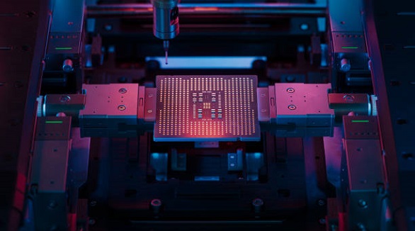
BGAs are vital for compact, high-functionality devices, but demand meticulous routing to overcome design challenges in reliability, manufacturability, and signal integrity.
 2025/09/11
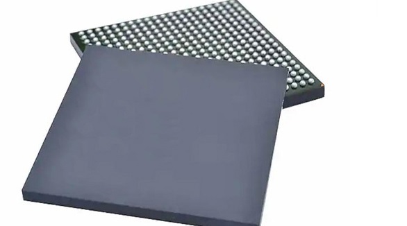
Compared to THT, SMT offers better miniaturization and weight reduction in any electronic application. With the use of BGA packages, high-assembly density, reliability, and improved performance are achieved; on the other hand, this requires a rework and inspection that is not really common. PCBX specializes in the area of advanced SMT and BGA assembly to help drive modern requirements of compact electronic devices.
2024/07/26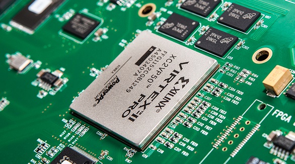
Ball Grid Array (BGA) components, such as PBGA, CBGA, CCGA, TBGA, and CSP, provide high I/O density, improved reliability, and high-quality electrical and thermal performance. Quality assembly and functionality are assured since advanced soldering and inspection methods are required, like AXI and AOI. Proper storage and handling shall guarantee the performance of the devices.
2024/07/26