
- Products & Capabilities

- About
- Resources
How to Mount a PCB for SMD LEDs


Learn how to mount a PCB for SMD LEDs — pad design, thermal vias, stencil printing, and reflow tips.
Surface-mount device (SMD) LEDs have become the default choice for lighting, indicator, and backlighting applications because of their compact size, efficient thermal characteristics, and compatibility with automated assembly. But an LED is only as good as the board it sits on. Poor mounting practices—wrong pad geometry, inadequate thermal relief, misapplied solder paste—can shorten LED lifespan, cause color shift, or lead to outright failure. This article walks through the key considerations for mounting a PCB for SMD LEDs, from board selection to reflow.
Choosing the Right Board Material
The starting point is picking a substrate that matches the thermal load of the LEDs. Low-power indicator LEDs (a few milliwatts to tens of milliwatts) can usually sit comfortably on standard FR-4. As power rises—into the range of high-brightness or high-power LEDs used in lighting fixtures—heat dissipation becomes the limiting factor, and metal-core PCBs (MCPCBs), typically aluminum-backed, are the more common choice. Aluminum substrates conduct heat away from the LED junction far more effectively than FR-4, which helps maintain consistent luminous output and color temperature over the product's life. For extremely high thermal density applications, copper-core boards or boards with embedded copper coins are sometimes used, though at a higher cost.

Pad Layout and Footprint Design
SMD LEDs come in standardized packages—common sizes include 0603, 0805, 1206, 3528, 5050, and larger high-power packages—and each manufacturer publishes a recommended land pattern in its datasheet. Following that footprint precisely matters more for LEDs than for many other passives, because pad size and spacing affect both solder joint reliability and thermal performance.
Key layout considerations include:
Pad size and spacing: Undersized pads increase thermal resistance and can cause tombstoning during reflow; oversized pads can cause the LED to shift during soldering.
Thermal pads: Many SMD LEDs, especially mid- and high-power packages, include a central thermal pad beneath the package. This pad should connect to a copper plane or thermal via array, not just a small isolated pad.
Polarity marking: SMD LEDs are polarity-sensitive. The silkscreen and pad design should make anode/cathode orientation unambiguous, since a reversed LED simply won't light and is easy to miss in a visual inspection on a densely populated board.
Solder mask design: A solder-mask-defined pad can help keep solder paste from spreading beyond the intended pad, which is useful for the tight tolerances typical of LED footprints.
Thermal Management: Vias and Copper
Because LED lifespan drops as junction temperature rises, thermal design isn't optional even for moderate-power applications. The most common approach is a thermal via array directly beneath (or immediately adjacent to) the LED's thermal pad, connecting the top copper layer to an internal or bottom copper plane that acts as a heat spreader.
A few practical points:
Via size and pitch should balance thermal conductivity against the risk of solder paste being wicked down into the via during reflow (a phenomenon sometimes called "via wicking" or "solder starvation"). Via-in-pad with plugging and capping is a common solution for high-power LED footprints.
Copper weight matters. Doubling copper thickness on the LED layer, or adding a heavier copper pour beneath the thermal pad, measurably reduces thermal resistance.
For MCPCBs, the dielectric layer between the copper circuit and the aluminum base is engineered specifically for thermal conductivity, so its thickness and material should be matched to the expected power dissipation rather than treated as an afterthought.
Solder Paste and Stencil Design
Stencil aperture design for SMD LEDs typically follows standard SMT stencil guidelines, but with attention to the thermal pad. For LEDs with a large exposed thermal pad, a single large stencil aperture can trap outgassing and produce voids under the pad, which in turn worsens heat transfer. Many assemblers instead use a windowpane or grid pattern of smaller apertures over the thermal pad, which distributes paste more evenly and reduces the risk of trapped air.
Paste volume also affects standoff height. Too little paste can leave the LED sitting unevenly, affecting light distribution and pattern-based optical designs; too much can cause solder to wick up the LED's side terminations.

Reflow Profile Considerations
SMD LEDs are sensitive components, and the reflow profile should follow the LED manufacturer's recommended thermal profile closely, including peak temperature, time above liquidus, and ramp rate. Exceeding the specified peak temperature or dwell time can degrade the LED's internal phosphor coating (in white LEDs), damage the encapsulant, or delaminate the die attach, none of which may be visible immediately but can shorten operational life or shift color output over time.
Because LEDs are often mixed on a board with other components that have different thermal mass, profiling the board as a whole—not just the LED footprint in isolation—helps confirm that every component sees an appropriate profile.
Placement Accuracy and Inspection
Pick-and-place accuracy matters more for LEDs than many passives, both because of polarity and because uneven placement can affect the light-emission angle in applications where multiple LEDs need to align optically (such as backlights or linear light bars). Post-reflow inspection—automated optical inspection (AOI) in particular—should check not just solder joint quality but also LED orientation and any visible tombstoning or tilt.
Mounting a PCB for SMD LEDs is less about following a single rule and more about matching several interacting factors—substrate choice, pad and via design, stencil pattern, and reflow profile—to the specific power level and optical requirements of the LED in question. Low-power indicator applications have considerable design margin, while high-power lighting applications require deliberate thermal engineering at every step, from copper weight to via structure to dielectric selection. Getting these fundamentals right at the design stage avoids costly rework and helps ensure the finished product performs consistently over its intended service life. As with most PCB engineering topics, PCBX aims to keep this kind of guidance grounded in practical, verifiable design fundamentals rather than generic advice, so readers can apply it directly to their own LED board designs.
Hot Tags:

Contact us

If you can't find what you're looking for, please contact us.
Article
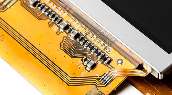
The LCD PCB interface is crucial for efficient, reliable displays, connecting control circuits to the display and impacting device performance and user experience.
 2025/10/30
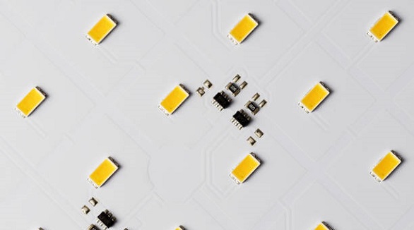
LED PCBs power modern lighting with efficiency and adaptability, ideal for diverse applications. Their design emphasizes thermal management, cost-effectiveness, and versatility, driving sustainable illumination solutions.
2024/11/21
Choose 1000 lumens for moderate brightness and energy efficiency in smaller spaces; opt for 1500 lumens for brighter coverage in larger areas.
2024/11/18