- Products & Capabilities

- About
- Resources
Board Plating vs. Hole Plating


Board and hole plating are essential PCB manufacturing processes, each serving unique roles in ensuring electrical connectivity, mechanical reliability, and overall product quality.
In the complex realm of printed circuit board (PCB) manufacturing, plating processes are critical to ensuring electrical connectivity, mechanical strength, and overall reliability of electronic devices. Board plating and hole plating are two significant processes used in this regard. Though both involve metal deposition on the PCB surface, they serve unique purposes and are conducted with distinct methodologies. Understanding these differences is critical to anyone engaged in PCB design, manufacture, or quality control.
Understanding Board Plating
Board plating, or panel or surface plating, is where the entire surface of a PCB panel is covered with a metallic layer. The metallic layer covers copper traces and substrate uniformly, which in production is crucial. The primary reason for board plating is to create a temporary conductive layer that facilitates other electroplating processes, ensuring electrical connectivity along the board at various stages.
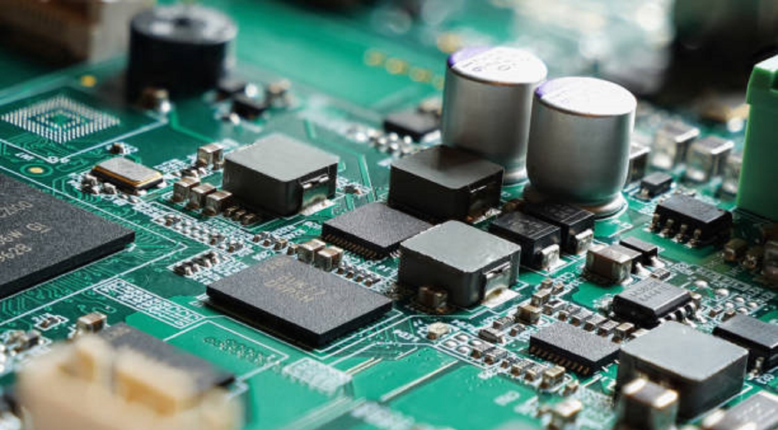
Copper is employed as the metal of choice due to its good conductivity and interfacing with the most widely used PCB material. The board is plated after copper foil is applied over the substrate and patterns for the circuit are set by photolithography and etching. Electroplating is applied to the panel to apply a uniform layer of metal. The conducting layer is removed selectively in final etching, leaving only the desired circuit traces and pads.
One key thing about board plating is that it is a transient process. Unlike liquid plating technologies that remain incorporated into the final product, board plating gets dissolved during later fabrication processes. It has the function of offering conductive paths needed in manufacturing but removing unwanted paths that would cause short circuits.
Knowing Hole Plating
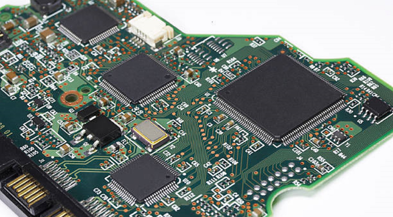
Alternatively, hole plating is used to treat the metallization of holes drilled through, vias, and other through-hole features. It is required for making electrical connections between layers of multilayer boards and for providing good, stable mounting points for through-hole components. Board plating, in contrast, is a feature and impacts the board's functionality and reliability indirectly.
Hole plating starts once drilling processes have produced the required holes and vias. The holes are initially provided with non-conductive walls, typically from a substrate such as fiberglass. For purposes of ensuring electrical continuity across layers, the walls must be made conductive.
The common process includes both electrolytic copper plating and electroless copper deposition. The electroless method deposits a thin copper layer chemically on the walls of the hole without any external current. Electrolytic plating continues to build up the copper thickness to specifications through this initial layer.
Copper thickness is crucial in hole plating since it affects both electrical performance and mechanical reliability. Standard requirement is generally described as 20 to 35 micrometers thick. Insufficient plating can lead to electrical discontinuities or thermal stress failure, while excess thickness can hinder component insertion or produce unwanted capacitive effects.
Key Differences in Application and Purpose
The primary difference between board and hole plating lies in their intended applications and durability. Board plating is an interim fabrication aid, whereas hole plating plays essential electrical and mechanical roles in the end product PCB. Designers give particular concern to hole plating requirements to provide for current-carrying capacity, thermal cycling, and mechanical stress requirements, which directly affect performance and reliability.
Board plating specifications are generally related to requirements within the manufacturing process and not the final product. The procedures also vary in timing within the manufacturing order. Board plating usually takes place early, sometimes even prior to finishing the final patterning of the circuit, whereas hole plating takes place after drilling and can be combined with other finishing procedures near the end of fabrication.
Process Control and Quality Considerations
Board and hole plating both require tight process control to ensure quality and consistency. Surface uniformity is critical in board plating because differences can lead to process flaws. Control is focused on bath chemistry, current density, and plating time.
Hole plating quality control is more complex since it is in three dimensions. Length variability in holes requires precise thickness measurement. Throw power, or the ability to deposit metal evenly in recessed surfaces, is a critical issue in hole plating and of secondary importance in board plating.
Economic and Environmental Considerations
The economic impact of board and hole plating is considerable. Board plating takes more solution volume and processing time. Although most of it is stripped later, it entails material loss and disposal problems. Hole plating, however, taking less material, demands costly precision, especially in the process of electroless copper. The fixtivity of hole plating ensures that defects formed after plating render boards unusable, making reliability essential.
Environmental considerations include plating waste disposal, chemical waste disposal, and energy consumption. Waste disposal differs due to each process having a different chemistry.
Future Trends and Developments
With advancing PCB technology in terms of higher densities and finer geometries, both hole and board plating operations are changing. New materials, improved controls, and new chemistries are emerging to meet the demands of modern manufacturing. For hole plating, lower environmental impact direct metallization processes are finding increasing usage. Meanwhile, board plating is being designed to accommodate new substrates and complex shapes.
In conclusion, while board and hole plating might appear to be equal terms, their roles, applications, and impacts on the manufacturing of a PCB and the functioning of a PCB are fundamentally different. Board plating enables short-term manufacturing, while hole plating enables essential, long-term circuit connections. Understanding these differences is crucial in making smart design decisions, effective process control, and producing high-quality electronic devices.
Hot Tags:

Contact us

If you can't find what you're looking for, please contact us.
Article
Button plating in flex PCBs enhances flexibility, reliability, and miniaturization, meeting modern design demands for smaller, highly functional devices.
 2025/01/06
Mounting holes in PCBs ensure mechanical stability, electrical functionality, and thermal management, crucial for design integrity and performance.
2024/11/05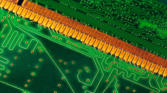
PCB side plating, or edge plating, involves copper along PCB edges, enhancing connectivity, conductivity, shock protection, and assembly, especially for small boards. Used in Wi-Fi and Bluetooth modules, it improves signal quality and EMC. Limitations include necessary design gaps and exclusion of V-cuts.
2024/08/21