- Products & Capabilities

- About
- Resources
How to Choose Standard Via Drill Sizes


Proper via drill sizes in PCB design are crucial for performance, cost, and manufacturability, considering electrical needs, space, and manufacturer guidelines.
Printed Circuit Boards (PCBs) constitute the pieces on which the pieces of today's electronic items are built. PCB performance as well as manufacturability depend, in some key respects, upon using proper via drill sizes. Vias represent plated holes with very small dimensions, where electric connections from layer to layer within a PCB exist. This article explains the selection of standard via drill sizes for your PCB design in view of manufacturability, cost, electrical performance, and general structural integrity.
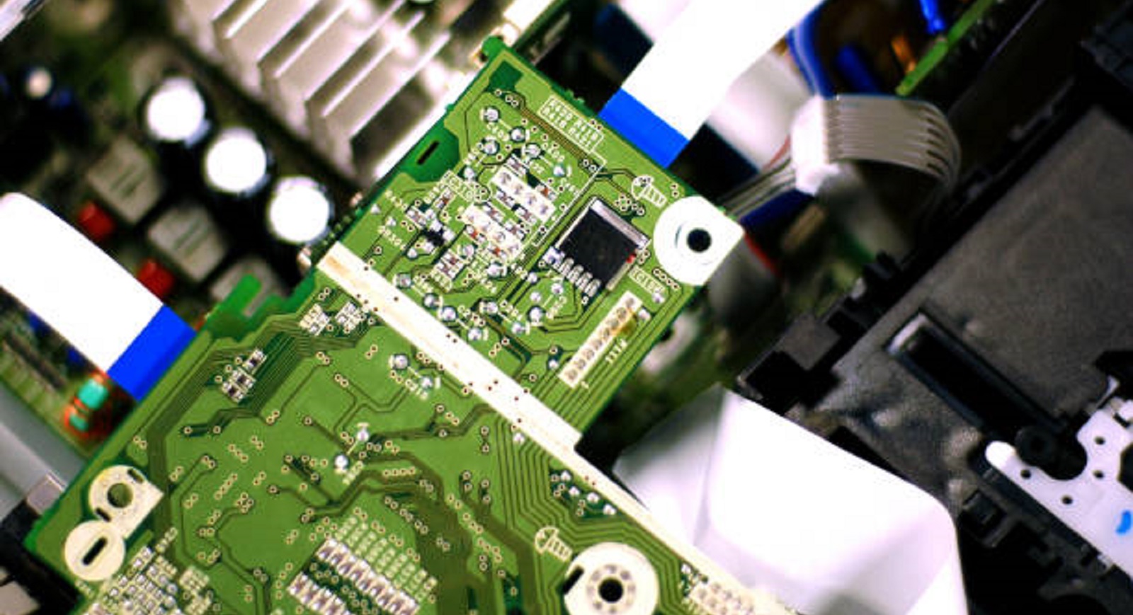
Understanding PCB Vias
On a PCB, the via serves to offer connectivity from layer-to-layer. Three are the chief types of vias:
Through-Hole Vias: These pass from top layer to bottom layer and connect each layer in between. They are the most affordable and simplest via.
Blind Vias: These are used to connect an outer plane to one or more inner planes but don't traverse the board. Blind vias take up less room on the PCB layout, especially valuable in high-density layouts.
Buried Vias: They are fully contained within the inner layers and don't appear on the surface. Buried vias add process complexity and expense but can be necessary for complex multi-layer designs.
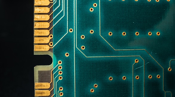
Importance of Via Drill Size
Choosing the correct via drill size is important since it impacts the electrical performance, manufacturability, structural integrity, and cost of the PCB. Even good PCB layouts must place manufacturability first since a design is useless if not easily producible.
Important Considerations:
Cost and Manufacturability: Different PCB manufacturers have different preferred drill sizes, generally providing a set of standard sizes. Inasmuch as there is no standard drill size, sizes such as 0.6mm are typically applied. Uniform via sizes across the board can ease fabrication, decrease costs, and minimize errors.
Electrical and Thermal Performance: Via size plays a significant role in electrical behavior and thermal management. More current can be handled by larger vias, which is crucial in power distribution networks but may bring about additional capacitance that affects signal integrity. Via sizes are selected by designers weighing current-carrying requirements and signal integrity.
Space and Density Limitations: In the case of high component-density PCBs, space limitations often dictate the need for small via sizes. Microvias, which are smaller than usual vias, are used in HDI designs to save space but require advanced, costly manufacturing processes.
Board and Component Issues: Board thickness and components may have a bearing on via size selection. The aspect ratio—via diameter to board thickness—should be in line with manufacturer requirements to ensure uniform plating.
Via Selection and Optimization Procedures
Utilize Manufacturer Guidelines: Take note of your PCB manufacturer's rules and guidelines. They typically have pre-defined standard drill sizes rules that can ease your design and minimize risks.
Use IPC Standards: Standards like IPC-2222 offer PCB design recommendations, e.g., minimum hole diameters as a function of pad diameter, to ensure your via parameters are at industry standards and best practice.
Minimize Via Count: While required for connection, excessive vias can affect mechanical properties and increase costs. Good via placement can reduce effects while still fulfilling design needs without making the layout overly complex.
Space Optimization and Trace Width: Trace design is not independent of via routing. Optimal trace design can reduce the number of vias required, lowering impedance and electromagnetic interference (EMI) issues.
Involve Manufacturers Early: Early communication with your fabricator can align your design requirements with their manufacturing capabilities, specifically in aspect ratios, minimum hole diameters, and drilling capacity.
Calculation and Size Recommendations
How to Calculate Via Drill Sizes
Define Lead Diameter: Start by identifying the lead diameter of your components, usually provided on datasheets.
Approximate Minimum Hole Size: Use this formula:
Minimum Finished Hole Size = Lead Diameter + 0.25mm
Approximate Pad Diameter: According to your minimum hole size, make an estimate of the pad diameter. Pads usually should be slightly larger than the hole so that they can add mechanical strength and proper soldering.
Size Guidelines: Generally, through sizes start at 0.15mm for microvias and up to 0.6mm for regular through-hole vias. The dimension is based on current demand, board design complexity, and production capabilities.

Selection of appropriate via drill sizes is an extremely critical activity in PCB design that has straight-forward consequences for board performance, cost, and manufacturability. Taking into consideration the elements of manufacturability, electrical performance, space availability, and consulting with manufacturers of PCB, designers can make informed decisions leading to overall improvement in quality and efficiency of PCB projects.
We at PCBX understand that PCB design complexity may be overwhelming. With our vast experience, we ensure that you have tailored solutions at your beckon to help navigate you through the hurdle so your projects become a success from the design phase all the way through production.
Hot Tags:

Contact us

If you can't find what you're looking for, please contact us.
Article
Vias in PCBs connect multiple layers and come in types like through-hole, microvias, blind, and buried. Proper sizing and design optimize PCB performance and reliability, aiding advanced device development.
 2024/10/16
PCBs are central to electronic devices, featuring holes and vias critical for functionality. Holes, like through-holes and mounting holes, serve electrical or mechanical purposes, while vias ensure electrical connections across PCB layers. Understanding their differences is key for optimal performance, reliability, and manufacturability in PCB design.
2024/09/11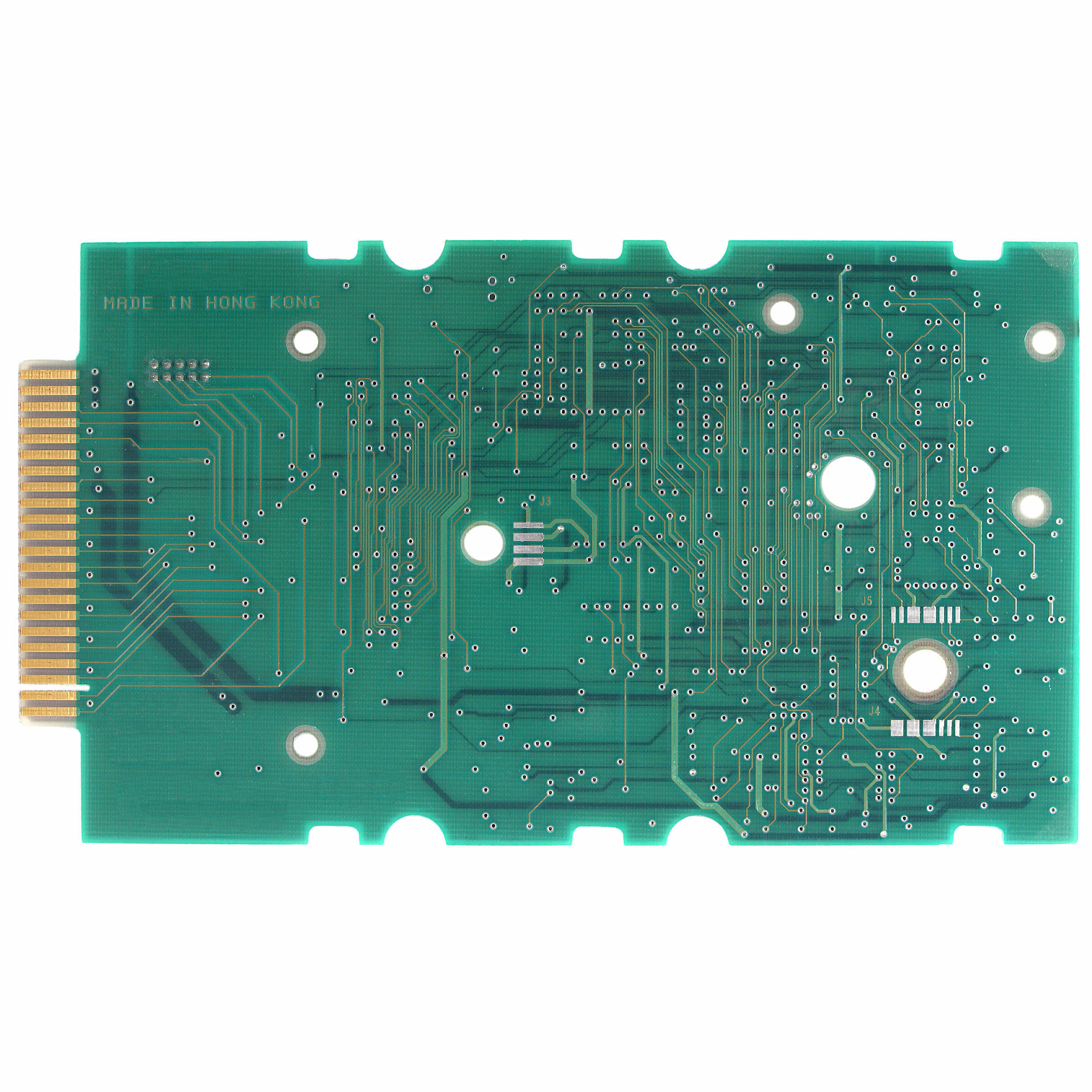
Backdrill in PCBs removes stubs in vias to improve signal integrity and impedance control, crucial for high-frequency, multilayer boards. It’s vital in communication, servers, medical, and aerospace applications.
2024/08/01