- Products & Capabilities

- About
- Resources
What is Transistor Inverter Circuit?


Transistor inverter circuits are vital in converting digital signals and limited power sources into reliable energy, enabling consistent performance in various applications despite power outages.
Electric power is undependable in most locations, with remote villages and even urban areas experiencing frequent power outages. These outages are particularly inconvenient when power is needed the most. But the remedy for such situations is in the subtle but powerful technology of transistor inverter circuits, which have a most significant application in both digital and power electronics. They offer a transformative way to convert limited power sources into reliable energy, enabling consistent performance across various applications.
Understanding Transistor Inverter Circuits
A transistor inverter circuit is a simple electronic circuit that is employed to invert a digital input signal to its opposing logic level at the output. The function of inversion in digital systems is needed for signal inversion, buffering, logic level translation, clock generation, and numerous other applications. With the ability to achieve high-speed operation and maintain high power efficiency, transistor inverters are crucial in applications ranging from microprocessors to power management systems.
Core Components and Functioning
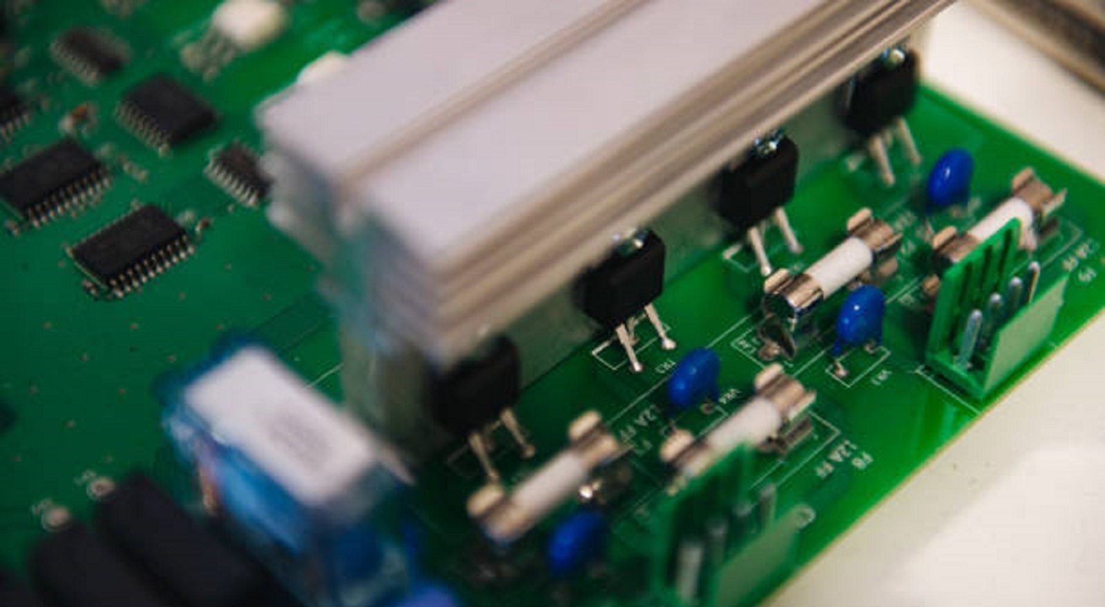
Transistor inverter circuits utilize a transistor, configured to switch states, to manage signal inversion. The two commonly used transistors are the Bipolar Junction Transistor (BJT) and the Metal-Oxide-Semiconductor Field-Effect Transistor (MOSFET). Let us discuss how these components work:
BJT Inverter Circuit:
A BJT inverter operates using a single BJT; when the input is low, the transistor is off, and the output is high due to the load resistor. Conversely, a high input turns the transistor on, drawing the output low via the collector-emitter route. Although cost-effective, BJTs are slower in performance compared to charge storage needs.
MOSFET Inverter Circuit:
On the other hand, MOSFET inverters are faster by avoiding the minority carrier issues faced with BJTs. Here, when the input voltage drops below the threshold, the MOSFET remains off, and the output is high. Crossing the threshold turns the device on, representing output low successfully. Mosfets are used for high-speed digital circuits due to quick switching and low power consumption.
CMOS Inverter:
Using complementary PMOS and NMOS transistors, CMOS inverters invert with high efficiency. PMOS is on at low input and pulls the output high while NMOS is off. NMOS is turned on by a high input, pulling the output low while PMOS is off. With low power consumption from the fact that there is no current flow between supply rails under the static condition, this arrangement is prevalent in modern integrated circuits.
Application in Power Inversion
Transistor inverter circuits are outstanding in power conversion equipment, especially where the supply of electricity is irregular. In remote or off-grid locations, a transitor-based inverter can effectively invert a 12V DC battery supply to a 220V AC supply for household use. The inversion provides a stable power supply for essential equipment during outages.
Oscillation Control: A multivibrator circuit comprising switching transistors produces controlled oscillations needed for the conversion process.
Stabilization Elements: A regulated power supply comprising BJTs and diodes stabilizes the oscillations for a steady frequency output.
Transformation Mechanism: An AC transformer steps up the oscillated output to the necessary voltage level, enabling compatibility with household AC devices.
Such circuits can be part of miniature home generators, alleviating power deficits in rural electrification schemes.
Key Design Criteria
Designing a good transistor inverter circuit means paying serious attention to some very important considerations:
Propagation Delay: This measure affects speed and the ability of the inverter to switch states rapidly after input transitions. The reduction of propagation delay is of serious concern for high-speed applications.
Gain and Signal Integrity: In order to supply useful logic levels, an inverter should possess a gain in excess of one to maintain strong noise margins along with clean signal transitions.
Fan-out Capacity: This refers to the ability of the inverter to drive more than a single component without degrading the signal, extremely vital in complex circuit designs.
Power Efficiency: Especially in battery or portable equipment, power consumption should be kept at a minimum. CMOS inverters excel in this area since they have low quiescent power consumption.
Noise Immunity: It is important that the inverter can perform well under electrically noisy environments. Schmitt trigger inverters, for example, help reject noise from input waveforms.
Variety of Applications
Transistor inverter circuits have diverse applications across a range of fields:
Digital Logic: They are an integral part of the creation of logic gates, providing elementary functions such as NOT, NAND, and NOR gates significant in computer systems.
Communication Systems: Inverters are used in signal modulation and frequency generation, enhancing the integrity of signal transmission.
Power Systems: They facilitate renewable energy systems, for instance, from DC of solar panels to useful AC power.
Signal Interface and Conversion: Inverters help in signal interfacing between various logic levels, making systems more compatible.
Transistor inverter circuits are not simply electronic devices; they are essential solutions bridging gaps in both digital processing and power conversion. Through learning and working with these circuits, it becomes possible to create novel solutions to real-world issues such as power reliability in marginalized communities. Their ability to transform constrained power sources to viable energy renders them highly valuable in pushing the limits of what can be achieved by electronic systems, and as such, they continue to be an integral component of contemporary technology innovation.
Hot Tags:

Contact us

If you can't find what you're looking for, please contact us.
Article
Capacitive circuits store and release energy, stabilize voltage, filter signals, and manage power flow, making them vital for modern electronic systems.
 2024/12/11
Burn-in boards are vital for testing semiconductor reliability, simulating stress to reveal defects, ensuring high-quality devices before mass production.
2024/12/06
Carrier PCBs are crucial for data modulation, multiplexing, and network integration, supporting efficient and robust telecom infrastructures globally.
2024/12/06