

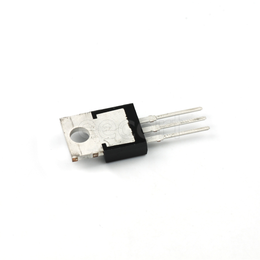
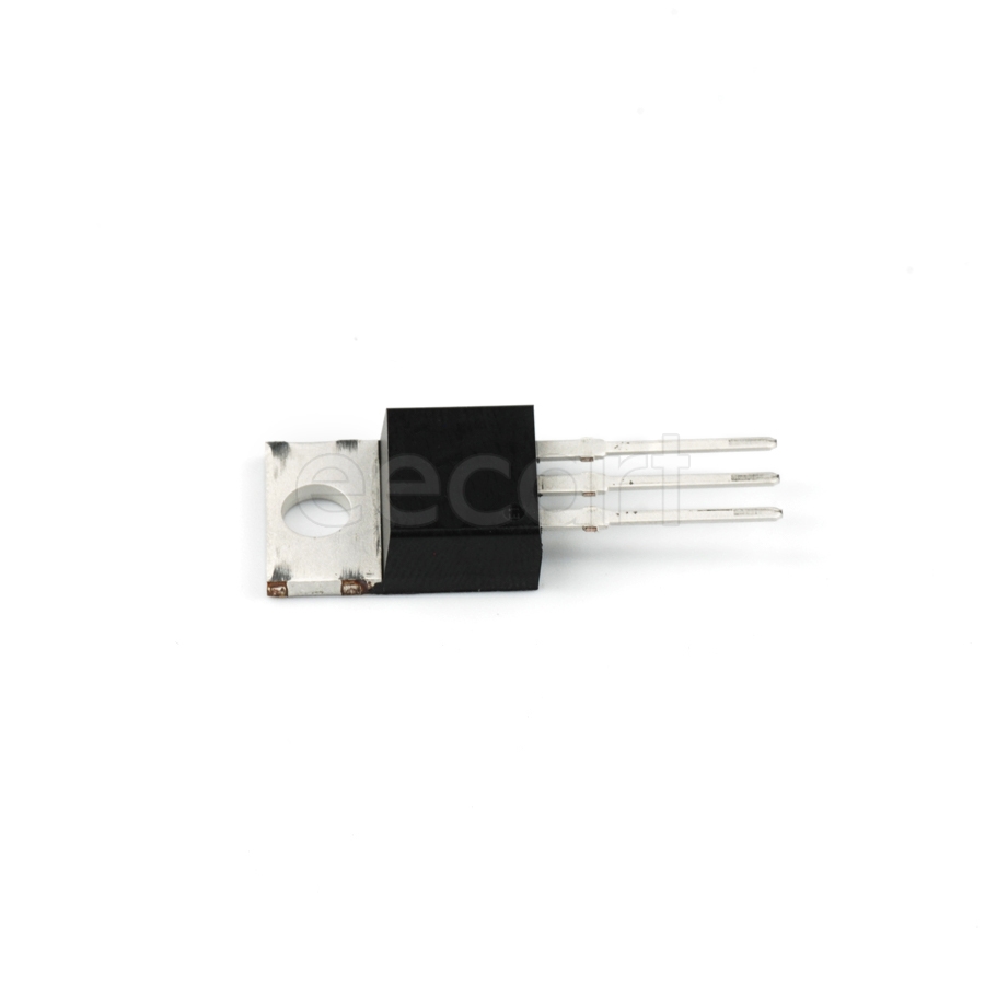
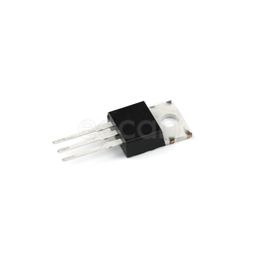
IRLB8721PBF
Manufacturer:
Infineon
Mfr.Part #:
IRLB8721PBF
Datasheet:

Description:
MOSFETs TO-220-3 Through Hole N-Channel number of channels:1 65 W 30 V Continuous Drain Current (ID):62 A 7.6 nC
| Parameter | Value |
|---|---|
| Length | 10.668 mm |
| Width | 4.826 mm |
| Termination | Through Hole |
| Max Operating Temperature | 175 °C |
| Min Operating Temperature | -55 °C |
| Number of Pins | 3 |
| Resistance | 8.7 mΩ |
| Height | 9.02 mm |
| Packaging | Tube |
| Lead Free | Lead Free |
| Radiation Hardening | No |
| RoHS | Compliant |
| REACH SVHC | No SVHC |
| Contact Plating | Tin |
| Lifecycle Status | Production (Last Updated: 10 months ago) |
| Max Power Dissipation | 65 W |
| Power Dissipation | 65 W |
| Threshold Voltage | 1.8 V |
| Number of Channels | 1 |
| Input capacitance | 1.077 nF |
| Continuous Drain Current (ID) | 62 A |
| Rds On Max | 8.7 mΩ |
| Drain to Source Voltage (Vdss) | 30 V |
| FET Type(Transistor Polarity) | N-Channel |
| Turn-On Delay Time | 9.1 ns |
| Turn-Off Delay Time | 9 ns |
| Element Configuration | Single |
| Rise Time | 93 ns |
| Dual Supply Voltage | 30 V |
| Gate Charge | 7.6 nC |
| Drain to Source Resistance | 16 mΩ |
| Max Junction Temperature (Tj) | 175 °C |
| Nominal Vgs | 1.8 V |
| Recovery Time | 24 ns |
| Gate to Source Voltage (Vgs) | 20 V |
| Drain to Source Breakdown Voltage (Vds) | 30 V |
| On-State Resistance | 8.7 mΩ |
| Schedule B | 8541290080 |
| Package Quantity | 1000 |
| Gate to Source Threshold Voltage | 1.8 V |
Out of Stock
Distributors --
--
--Unit Price$--
Ext.Price$--
| Qty | Unit Price | Ext.Price |
|---|---|---|
No data | ||