KICAD Design Tutorial
KiCAD PCB Design Tutorial
KiCad is a comprehensive, open-source software suite for electronic design automation (EDA). It provides an integrated environment to facilitate the entire workflow of designing and manufacturing electronic hardware, from circuit schematics to printed circuit boards.
KiCad has matured into a robust and capable electronic design automation (EDA) suite, making it suitable for the successful development and maintenance of complex electronic boards. It does not impose any practical limitations on board size, supporting up to 32 copper layers, 14 technical layers, and 4 auxiliary layers.
As an open-source project licensed under the GPL, KiCad represents an ideal tool for open hardware projects where transparency and community involvement are important. Its lack of licensing fees or restrictive terms makes it an accessible and cost-effective solution for engineers, hobbyists, and small businesses alike.
The comprehensive feature set, scalability, and open-source nature of KiCad have contributed to its growing popularity and adoption for a variety of electronic design endeavors, from simple hobbyist projects to sophisticated commercial products.

Drawing Electronic Schematics
1.Launch the KiCad application on your computer.
This will open the main project manager window.From the KiCad project manager, you can access the suite's eight integrated software tools:Eeschema,Schematic Library Editor,Pcbnew,PCB Footprint Editor,GerbView,Bitmap2Component,PCB Calculator,Pl Editor.
2.Build a new projec:
Open the KiCad Project Manager by launching the KiCad application.
In the Project Manager, click on the "File" menu and select "New Project".
In the "New Project" dialog, choose a location on your file system to save the new project. It's a good idea to create a new folder for each project.
Enter a name for your new project and click "Save".
The Project Manager will now show your new project. You can access the various KiCad tools from the toolbar or by right-clicking on the project name.
3. Let's begin by creating a schematic. Start the schematic editor Eeschema  . It is the first button from the left.
4. Click on the Page Settings icon 
Here are the steps to set the page size and title for a new schematic in KiCad:
- Open the Eeschema schematic editor from the KiCad Project Manager.
- In the Eeschema window, go to the "Page Layout Editor" by clicking the icon on the toolbar or navigating to Preferences > Page Layout Editor.
- In the Page Layout Editor, set the "Paper Size" to "A4" from the dropdown menu.
- In the "Title Block" section, enter "Tutorial1" as the title.
- Click "OK" to apply the page size and title settings.
- These settings will now be reflected at the bottom right corner of your schematic sheet in Eeschema.
- Use the mouse wheel to zoom in and out of the schematic as needed.
- When you're ready, save the entire schematic project by going to File > Save Schematic Project in the Eeschema window.
5. Click on the Place Component icon in the right toolbar to place your first component in Kicad
6. Here are the steps to place a resistor component in your KiCad schematic:
In the Eeschema schematic editor, click on the middle of your schematic sheet to position the cursor.
This will open the "Choose Component" window.
In the component search field, type "R" to filter the list and find resistor components.
You'll notice the "Resistor" entry has a "Device" heading above it. This indicates the library where the resistor component is located.
The "Resistor" component is part of KiCad's generic and widely-used library, making it a convenient choice for your design.
Select the desired resistor component from the list by double-clicking on it or highlighting it and clicking "Place".
The resistor symbol will now be placed on your schematic sheet, ready for you to customize its properties, such as the resistance value, power rating, etc.
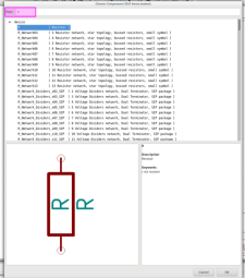
7.By double-clicking on the resistor component in the "Choose Component" window, you confirm your selection and close the window, allowing you to then place the component on the schematic sheet.
This two-step process of selecting the component in the "Choose Component" window, and then clicking on the schematic sheet to place it, gives you precise control over the placement of the components in your design.
Remember, you can always adjust the position of the component later by simply clicking and dragging it to a new location on the schematic sheet.
8.Zoom and pan the view in the KiCad Eeschema schematic editor:
- In the Eeschema window, locate the magnifier icon on the toolbar.
- Click on the magnifier icon to activate the zoom function.
- Left-click and drag the mouse to draw a zoom box around the area you want to focus on. Eeschema will then zoom in to that selected region.
- Scroll the mouse wheel forward to zoom in on the schematic.
- Scroll the mouse wheel backward to zoom out.
- Press and hold the middle mouse button (the mouse wheel).
- While holding the middle button, move the mouse to pan the view in the desired direction.
The combination of using the magnifier tool, mouse wheel scrolling, and middle-button panning allows you to easily navigate and inspect different areas of your schematic diagram in detail.
9.Rotate a component in the KiCad Eeschema schematic editor:
- In the Eeschema window, locate the resistor component (or any other component) you want to rotate.
- Hover the mouse cursor over the resistor component.
- Without clicking on the component, press the "r" key on your keyboard.
- The resistor component will immediately rotate 90 degrees clockwise.
This rotation functionality works for any component placed on the schematic sheet. You can repeatedly press the "r" key while the mouse is hovering over the component to rotate it in 90-degree increments.
10.Here's how to edit the value of a component in the KiCad Eeschema schematic editor:
- Locate the component on the schematic that you want to edit, such as a resistor.
- Right-click on the middle of the component to open the component's context menu.
- From the menu, select "Edit Component" and then choose "Value" to open the value edit dialog.
Alternatively, you can use keyboard shortcuts:
- Hover the mouse cursor over the component you want to edit.
- Press the "v" key on your keyboard to directly open the value edit dialog for that component.
Additionally, you can access the component's full edit window by pressing the "e" key while the cursor is hovering over the component.
- Notice that the right-click context menu displays the corresponding keyboard shortcuts for each available action, such as "v" for Value and "e" for Edit.
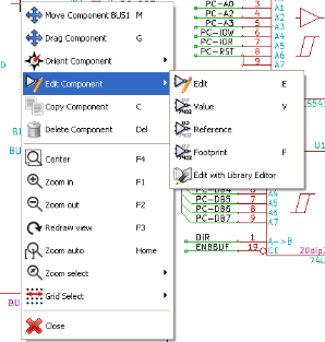
11. The Component value window will show up. Replace the current value R with 1 k. Click OK.

12. How to add another resistor component to your KiCad Eeschema schematic:
l With your schematic editor open, locate the toolbar at the top of the window.
l Look for the "Add Component" button, which may be represented by a graphical icon of a component.
l Click the "Add Component" button to open the Component Selection window.
l In the Component Selection window, find and select the resistor component you want to place.
l With the resistor component selected, move your mouse cursor to the location on the schematic where you want to place the new resistor.
l Left-click the mouse to place the resistor component at the desired position on the schematic.
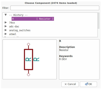
13.The resistor component you previously selected is now listed in the "History" section of the Component Selection window, appearing as "R". You can click the "OK" button to confirm the selection, and then left-click on the schematic to place the resistor component at the desired location.
14.Here are a couple of ways to delete a component from your KiCad Eeschema schematic:
Right-click on the component you want to remove:
- Locate the component on the schematic that you want to delete.
- Right-click directly on the component.
- From the context menu that appears, select the "Delete Component" option.
- This will remove the selected component from the schematic.
Use the keyboard shortcut:
- Hover the mouse cursor over the component you want to delete.
- Press the "del" or "delete" key on your keyboard.
- The component under the cursor will be removed from the schematic.
15.Duplicate a component in your KiCad Eeschema schematic:
- Locate the component on the schematic that you want to duplicate.
- Position your mouse cursor over the component you want to copy.
- Press the "c" key on your keyboard.
- With the duplicate component selected, move your mouse cursor to the desired position where you want to place the new component.
- Left-click the mouse to drop the duplicate component at the new location.
16. Right click on the second resistor. Select Drag Component. Reposition the component and left click to drop.
Here's how you can move a component in your KiCad Eeschema schematic:
- Locate the component you want to reposition on the schematic.
- Right-click directly on the component to open the component's context menu.
- From the menu options, select "Drag Component".
- With the "Drag Component" mode active, move your mouse cursor to the new desired location for the component.
- Left-click the mouse to drop the component and place it at the new position on the schematic.
This process allows you to easily relocate components within your circuit diagram. The right-click context menu provides the "Drag Component" option, which enables you to click and drag the component to a new position.
17. Change the grid size.
To change the grid size in the KiCad Eeschema schematic editor, follow these steps:
- Open your schematic in the KiCad Eeschema environment.
- Look for the grid size controls, which are typically located in the toolbar at the top of the Eeschema window.
- You should see a dropdown or input field that displays the current grid size, such as "1 mil" or "2.54 mm".
- Click on the grid size control to open the grid size selection menu.
- In the menu, you will find various grid size options to choose from, such as:
0.1 mm
0.5 mm
1 mm
2.54 mm (default)
1 mil
5 mil
10 mil
Select the desired grid size that best suits your design needs.
The grid on the schematic will instantly update to reflect the new grid size you have chosen.
18.To add a component from a library that isn't configured in the default project in KiCad, follow these steps:
- Open your KiCad project and go to the Eeschema (schematic editor) environment.
- In the left-hand panel, locate the "Library Browser" window.
- Click the "Add Component" button (usually represented by a "+" icon) in the Library Browser.
- In the "Add Component" dialog box that appears, you'll see a list of the available component libraries.
- If the library you need is not listed, you'll need to add it to the project. To do this, click the "Browse Libraries" button.
- In the "Library Manager" window, click the "Add Library" button.
- In the "Add EESchema Library" dialog, you can either:
a. Browse your local file system to select the library file (usually a .lib or .dcm file).
b. Specify the path to the library file directly.
- Once you've added the library, it should now appear in the list of available libraries in the "Add Component" dialog.
- Select the library containing the component you want to add, then navigate through the library contents to find the specific component.
- Double-click the component or select it and click "Add Component" to place it on your schematic.
20.To create a Bill of Materials (BOM) in KiCad, follow these steps:
- Open your KiCad project and go to the Eeschema (schematic editor) environment.
- In the top menu, go to Tools > Generate Bill of Materials.
- The "Bill of Materials" dialog window will appear, with various options and settings for generating the BOM.
- In the "BOM Generators" section, select the desired output format for your BOM, such as:
CSV (Comma Separated Values)
XML
HTML
- Customize the BOM settings as needed:
- Select the components to include in the BOM (e.g., all components, components with a specific property or field value).
- Choose the information to include in the BOM (e.g., component references, descriptions, values, quantities).
- Specify the order and grouping of the BOM entries (e.g., by component type, by manufacturer, alphabetically).
- Click the "Generate BOM" button to create the BOM file.
- The BOM file will be saved in the directory specified in the "Output Directory" field. The file name will be based on the selected output format (e.g., "my_project_bom.csv", "my_project_bom.html").
- You can now open the generated BOM file with a spreadsheet application, text editor, or web browser, depending on the output format you chose.
Here is the BOM Sample from pcbx

Kicad Layout Printed Circuit Board
1.To create a PCB layout in KiCad, follow these steps:
- Open your KiCad project and navigate to the Project Manager.
- In the Project Manager, click on the "Pcbnew" icon to open the PCB editor.
- If you encounter an error message stating that a *.kicad_pcb file does not exist and asks if you want to create it, simply click "Yes" to proceed.
The *.kicad_pcb file is the file format used by KiCad to store the PCB layout data. If this file does not exist, it means you are creating a new PCB layout for your project.
- The Pcbnew window will now open, presenting you with a blank PCB layout canvas.
This is where you will place the components, route the traces, and design the physical layout of your printed circuit board.
- From this point, you can start placing components, drawing tracks, and defining the PCB layers and dimensions according to your project requirements.
You can use the various tools and commands available in the Pcbnew interface to perform these tasks.
1. Begin by entering some schematic information. Click on the Page settings icon on the top toolbar. Set paper size as A4 and title as XXX
2.Open your KiCad project and navigate to the Pcbnew (PCB Editor) environment.
In the top menu, go to Design Rules > Design Rules.
The "Design Rules" dialog window will appear. Make sure the "Net Classes Editor" tab is selected.
In the "Net Classes Editor" tab, you can customize the design rule settings for your PCB.
In the "Clearance" field, set the value to 0.25 mm. This clearance setting determines the minimum spacing between tracks and between tracks and pads/vias.
In the "Track Width" field, set the value to 0.25 mm. This setting defines the minimum width for the copper tracks on your PCB.
These values of 0.25 mm for both clearance and minimum track width are generally a good starting point, as they are commonly used and supported by many PCB manufacturers.
Ensure that the measurements are in millimeters (mm), as this is the standard unit used in KiCad.
By setting the clearance and minimum track width to 0.25 mm, you are configuring your PCB design to meet the typical requirements of most PCB manufacturers. This helps ensure that your PCB can be successfully fabricated and assembled.
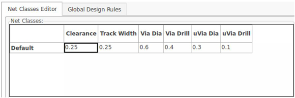
3. Click on the Global Design Rules tab and set Min track width to 0.25'. Click OK to commit your changes and close the Design Rules Editor window.
Setting the global design rules in KiCad's Pcbnew (PCB Editor):
Open your KiCad project and navigate to the Pcbnew (PCB Editor) environment.
In the top menu, go to Design Rules > Design Rules.
In the "Design Rules" dialog window, click on the "Global Design Rules" tab.
In the "Global Design Rules" tab, locate the "Minimum Track Width" field and set the value to 0.25.
This sets the global minimum track width for your PCB design to 0.25 units, which is typically millimeters (mm).
Once you've made the necessary changes, click "OK" to commit the design rule settings and close the "Design Rules Editor" window.
By setting the global minimum track width to 0.25 units, you are ensuring that all tracks on your PCB will have a minimum width of 0.25 units. This helps to meet the typical manufacturing requirements and ensures the feasibility of your PCB design.
4.Now we will import the netlist file. By importing the netlist file, you are linking the schematic design information (such as component placements and connections) to the PCB layout in Pcbnew. This ensures that the PCB design accurately reflects the schematic design, making the design process more efficient and reducing the likelihood of errors.
5. The ratsnest is a useful visual aid that helps you understand the connectivity of your PCB design before you start placing and routing the actual traces. By keeping the ratsnest visible, you can easily identify the connections between components and use this information to plan your PCB layout and routing process.
6. Moving components in KiCad's Pcbnew (PCB Editor):
- Open your KiCad project and navigate to the Pcbnew (PCB Editor) environment.
- In the PCB layout, identify the components you want to move.
- To move a component, hover your mouse cursor over the component you want to move.
- Press the "g" key on your keyboard while the component is selected.
- With the component selected, click and hold the left mouse button, then drag the component to the desired location on the PCB layout.
- Repeat steps 3-5 to move all the components around until you have minimized the number of wire crossovers in the ratsnest.
- The ratsnest visualizes the connections between the components, so minimizing wire crossovers can help optimize the layout and improve the overall routing of your PCB.
- Continue making modifications to the component placements until you have achieved an ideal PCB layout that meets your design requirements.

Once your custom circuit design is complete, you can generate Gerber files for each layer and send them to manufacturer for PCB production.
Steps to generate Gerber files in KiCad:
- Open your KiCad project and navigate to the Pcbnew (PCB Editor) environment.
- In the top menu, go to File > Plot to open the "Plot" dialog.
- In the "Plot" dialog, you will see a list of different layers that can be plotted as Gerber files.
- Configure the Gerber output settings:
Ensure that the "Plot mode" is set to "Gerber".
Select the layers you want to generate Gerber files for. Typically, this includes the following layers:
F.Cu (Front Copper)
B.Cu (Back Copper)
F.Silkscreen (Front Silkscreen)
B.Silkscreen (Back Silkscreen)
F.Mask (Front Solder Mask)
B.Mask (Back Solder Mask)
Edge.Cuts (Board Outline)
Set the "Gerber file option" to "Included" for each layer.
Optionally, you can set the "Plot scale" and other preferences based on your requirements.
- Click the "Plot" button to generate the Gerber files.
- By default, the Gerber files will be saved in the same directory as your KiCad project.
- Additionally, you can also generate a Drill file (containing the information about the drill holes):
In the "Plot" dialog, click on the "Generate Drill Files" button.
Configure the Drill file settings as needed and click "OK" to generate the Drill file.
After generating the Gerber and Drill files, you can provide these files to your PCB manufacturer, who will use them to fabricate your PCB.