Absolutely, the initial PCB layout and design phase is critical for determining both the cost and quality of the final product. By meticulously planning and adhering to best practices, you can avoid costly revisions and achieve optimal performance.
To ensure a successful start, we have compiled our PCB design guidelines, which serve as a comprehensive checklist.
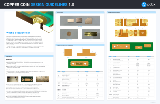
Multilayer PCB
Stackups and Impedances
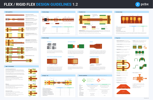
Flex / Rigid-Flex PCBs
Copper coin
Below are some key PCB design guidelines to consider:
1. Define Your Requirements
Functionality: Clarify the core functionalities the PCB must support.
Size and Shape: Determine the physical dimensions and shape constraints.
Layers: Decide on the number of layers based on complexity.
2. Component Selection
Placement: Place critical components first (e.g., microcontrollers, connectors) to optimize signal paths.
Orientation: Maintain consistent orientation for similar components to make assembly easier.
Clearances: Ensure adequate clearance between components for automated assembly.
3. Schematic Design
Symbol Libraries: Use accurate and verified symbol libraries for components.
Component Labels: Clearly label all components to avoid confusion during layout.
Net Naming: Use consistent and descriptive naming for nets to trace signal flow easily.
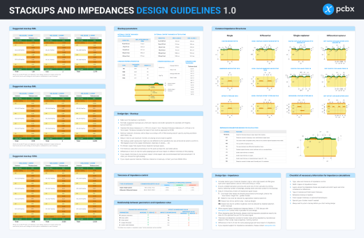
4. Layer Stack-up
Ground and Power Planes: Use dedicated layers for ground and power to improve signal integrity and reduce noise.
Signal Routing: Assign different layers for different signal types (analog, digital, power).
Thermal Considerations: Incorporate thermal vias and copper pours to manage heat dissipation.
5. Routing Guidelines
Trace Width and Spacing: Adhere to IPC standards for trace width and spacing based on current requirements.
Impedance Control: For high-speed signals, maintain controlled impedance by using appropriate trace dimensions and spacing.
Via Management: Minimize the use of vias to reduce signal reflection and path delay.
6. Power Distribution
Decoupling Capacitors: Place decoupling capacitors close to power pins of ICs to filter out noise.
Power Traces: Ensure power traces are wide enough to handle required current without excessive voltage drop.
7. Signal Integrity
Differential Pairs: Route differential pairs (e.g., for USB or Ethernet) close together and with equal length to maintain integrity.
Grounding: Maintain a continuous ground plane under high-speed signals to minimize EMI.
Terminations: Use proper termination resistors where needed to prevent signal reflection.
8. Design for Manufacturability (DFM)
Panelization: Optimize PCB panelization for efficient manufacturing and lower cost.
Assembly Checks: Design for easy component placement and soldering.
Test Points: Include test points for post-assembly testing to ensure functionality.
9. Thermal Management
Heat Sinks: Integrate heat sinks or thermal vias for components that generate significant heat.
Copper Pours: Use large copper pours to spread and dissipate heat.
10. Documentation
Gerber Files: Ensure all Gerber files are correctly generated and verified.
Assembly Drawings: Provide detailed assembly drawings and a Bill of Materials (BOM).
Design Rules Check (DRC): Perform a DRC to identify and correct rule violations before manufacturing.
11. Simulation and Testing
Simulations: Run electrical simulations to validate signal integrity and power distribution.
Prototyping: Create prototypes and validate them through rigorous testing before full-scale production.
By following these guidelines, you can enhance the overall design and functionality of your PCB, reduce costs, and accelerate the time-to-market for your product.