- Products & Capabilities

- About
- Resources
Common PCB Assembly Defects


Common PCB assembly defects, their root causes, and proven prevention methods are outlined to improve reliability, yield, and manufacturing efficiency.
As electronic products continue to evolve toward higher density, smaller form factors, and tighter tolerances, PCB assembly quality has become a hallmark in product reliability. Even a good printed circuit board may break down when assembly errors are brought during assembly of the board through soldering or by placing components. This article discusses the most frequently used PCB assembly defects, their causes, and offers effective, proven methods of reducing them based on enhanced process controls, inspections, and design-for-manufacturability (DFM) techniques.
The Importance of PCB Assembly Defects
The defects in PCB assembly are mistakes committed during the mounting/soldering of the components on the board. Such defects may result in electrical short-circuit, open circuit, intermittent failures, thermal instability or mechanical weakness. Even in a weak solder joint, failure of the system can occur in mission-critical applications like automotive electronics, medical devices or industrial controls.
In addition to reliability, issues in assembly directly affect manufacturing yield, production cost and time-to-market. It is crucial to find root causes early, and the processes must be designed in a way that they do not occur to achieve consistent, scalable production.
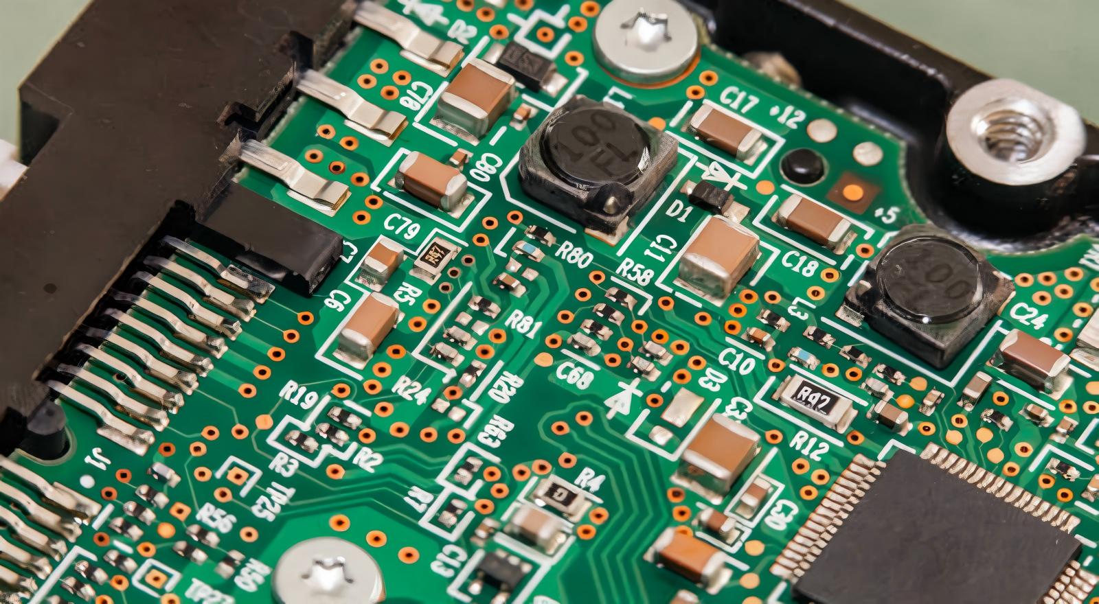
Common PCB Assembly Defect
Solder Bridging and Short Circuits
Solder bridging is a phenomenon that is caused by too much solder between neighboring pads, pins or traces, which are to be electrically isolated. This flaw is most prevalent in fine component parts and dense designs.
Primary causes include:
Splendor of solder paste when stenciling.
Poor distance between solder mask.
Weak alignment of the stencil or aperture design.
Suboptimal reflow profiles.
The short circuit of solder bridges may make a board unwound or act erratically especially in high-speed or mixed-signal circuits.
Weak Joints and Shortages of Solder
The lack of solder leads to inappropriate mechanical strength or electrical continuity of joints. These joints are usually skinny, incomplete or wetted wrongly.
Common contributors:
Stencil apertures that are undersized.
Poor transfer efficiency of paste.
Aged pads or component leads.
Lower than solder alloy reflow.
Vibration and thermal cycling are very sensitive to weak joints hence they cause a significant reliability risk in the industrial and automotive setting.
Open Solder Joints
Others are open solder joints which are defined as the failure of a component lead to establish an electrical connection with the PCB pad.
Typical causes:
Misalignment of components during assembly.
Inadequate solder volume
Lack of cleanliness on the surface or oxidation.
Lack of heat during reflow.
Open joints tend to lead to intermittent failures that can only manifest themselves after the environment is strained hence they are not easily diagnosed when subjected to tests.
Solder Balling and Residual Solder Particles
Small and unintended solder balls that occur on the PCB surface during reflow are called solder balls.
Why they occur:
Solder paste or PCB moisture contamination.
Rapid heating during reflow
Pad extrusion.
Surface contamination
The loosening solder balls may move and lead to latent short circuits and lead to reliability problems in small assemblies.
Tombstaning (Manhattan Effect)
Tombstoning is an occurrence when a small passive component, at the end of the component, spins off the pad in the reflow process making the component stand upright.
Root causes include:
Lopsided geometry of pads or copper asymmetry.
Unequal volumes of solder paste.
Loss of heat in the component unevenly.
The component breaks electrically and it causes instant functional failure.
Component Misalignment and Skew
This is a failure that is caused by placing the components in the circuit board in the wrong position.
Component misalignment occurs when components are not positioned at their centres, are rotated or moved off their marks.
Typical reasons:
Calibration errors in pick and place machine.
Corrupted PCB design/placement data.
Placement Solder paste movement.
PCB or component warpage
Misalignment may cause open joints, solder bridging or poor performance, particularly in RF and high-speed designs where the accuracy of placing the components is paramount.
Cold Solder Joints
Cold soldering joints are dull joints which are created when solder does not melt or flow.
Causes include:
Poor reflow temperatures.
Improper flux activation
Poor thermal transfer
The joints can work at the first stage but tend to fail early in life due to mechanical or thermal load.
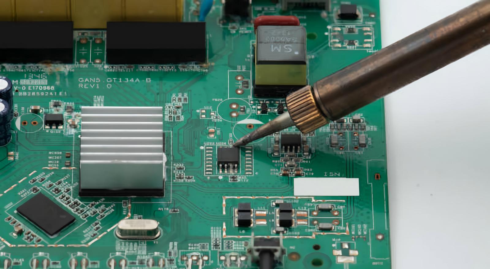
BGA and QFN Soldering Defects
BGAs and QFNs might have hidden solder joints, which may have an open, void, or head-in-pillow defect.
Contributing factors:
PCB or component warpage
Wrong quantity of solder paste.
Non homogenous thermal profiles.
These joints are not visible, and thus defects may not be felt without X-ray examination and thus risks on field failures are high.
Warpage and Its Effect on Assembly Defects
PCB and component warpage is also one of the significant contributors to solder opens, balling, and BGA defects. Unbalanced copper distribution, asymmetric stackups, uneven component placement and thermal gradients during reflow all affect warpage.
Mitigations measures involve:
Assigning balanced stackups of PCBs with equal copper layers.
Placing the elements in equal measures within the board.
Thermal relieving of large copper planes.
The choice of materials with low coefficient of thermal expansion (CTE).
Close coordination between the design, fabrication and assembly teams is essential in the reduction of the warpage risks.
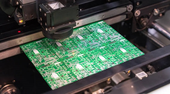
Best Practices to Eliminate PCB Assembly Defects
At PCBX, defect prevention is initiated by process discipline and early engineering involvement:
Maximize printing of solder paste using fine stencil design and humidity control.
Adjust reflow profiles depending on alloy, board thickness, and component combination.
Make sure that there is accuracy in placement with the help of fiducials and vision-assisted systems.
Use effective inspection such as AOI and X-ray of concealed joints.
Cleanliness and material control are to be observed to avoid oxidation and moisture problems.
To achieve a high level of reliability in products, prior to volume production, accelerated life testing and DFM validation reduce the risk even further.
Defects in PCB assembly can include solder bridging, solder insufficiency, open joints, misalignment, and warpage breakages, which are common but can be avoided to a great extent. It is important to develop reliable electronics by understanding their causes and mitigating them by designing thoughtfully, manufacturing under control and scrutinizing them during the manufacturing process.
Hot Tags:

Contact us

If you can't find what you're looking for, please contact us.
Article
FAI in SMT ensures product quality by detecting defects early, using methods like AOI and X-ray, ultimately enhancing efficiency and customer trust.
 2025/06/26
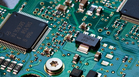
SMT assembly streamlines electronics manufacturing with compact, reliable designs using precise equipment, meeting high-density demands and international standards.
2024/10/29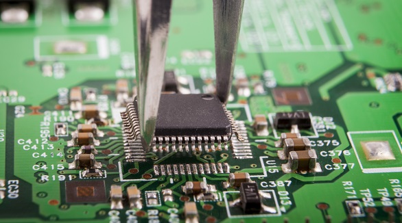
Still, SMT can further feature defects such as solder bridging, cold solder joints, tombstoning, and solder balling. Grasping the very common faults and their solutions is the key toward effective PCB assembly and reducing SMT errors—very much in line with the trend toward PCB miniaturization and higher component density.
2024/07/29