
- Products & Capabilities

- About
- Resources
PCBX.com Resources
Your source for industry knowledge, news, and expert insights

Latest Posts
Article

Learn what tenting via is in PCB fabrication, its working principle, benefits, limitations and differences from plugged and filled vias for circuit board design.
 2026/09/15

Learn which PCB components cannot use conformal coating. Avoid contact, thermal, optical & mechanical failures in industrial & automotive electronics.
2026/09/08
Learn how to mount a PCB for SMD LEDs — pad design, thermal vias, stencil printing, and reflow tips.
2026/09/03
Discover why DFM analysis matters in PCB design and how it prevents costly manufacturing errors.
2026/09/01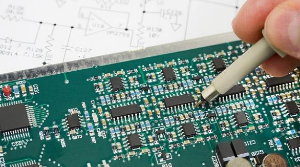
Learn core solder mask expansion DFM rules for PCB pads, vias and mask dam constraints to reduce defects and boost manufacturing yield.
2026/08/27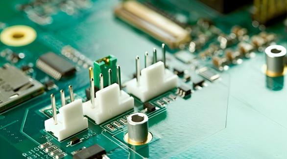
Key PCB routing rules for trace width, impedance control, via placement, plane integrity, and testability — practical guidance for reliable board design.
2026/08/25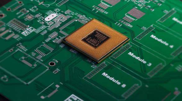
Learn multilayer PCB lamination process optimization, key strategies for reducing voids, warpage and improving inter‑layer reliability for high‑performance circuit boards.
2026/08/20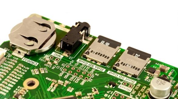
Learn practical strategies to cut PCB assembly cost, boost manufacturing efficiency, and avoid common production defects for electronic projects.
2026/08/18