- Products & Capabilities

- About
- Resources
Signal Reflection & Distortion in PCBs


Signal reflection and distortion, resulting from impedance mismatches, impact PCB performance and require strategic design, simulation, and material selection for mitigation.
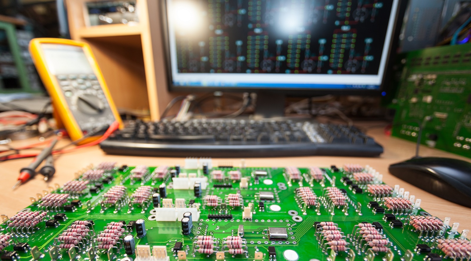
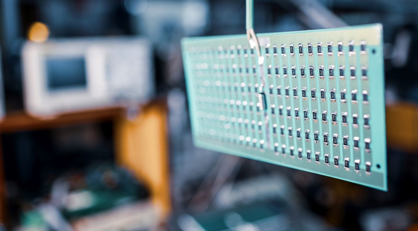
In the high-speed world of electronics, the printed circuit board (PCB) is the essential platform backing practically every electronic device. With the trend for devices to be quicker, smarter, and smaller, the challenges in designing circuits are also magnified. Some of the most apparent issues of engineers today are signal reflection and distortion. They are catastrophic to signal integrity (SI), leading to data error, synchronization issues, and overall compromised reliability of electronic systems.
Signal Reflection
Signal reflection in PCBs occurs when a traveling signal encounters an impedance mismatch along its path. They can occur due to line width variations, component to component changes, vias, or connectors. When such a mismatch occurs, some part of the signal energy reflects back towards the source, rather than moving to the destination. This reflection is measured by the reflection coefficient, a parameter that measures the degree of reflection; the higher the coefficient, the greater the reflection, and the lesser the coefficient, the less reflection.
Reflection is a fundamental issue in wired and wireless networks, manifesting as echoes that result in distortion, attenuation of the signal, and a rise in error rates. In high-speed and dense PCBs, in which components are reduced in size, and routing complexity grows, impedance matching as required becomes increasingly difficult.
Causes of Signal Reflection
The fundamental cause of signal reflection is an impedance mismatch along the transmission route. This mismatch can occur due to:
Changes in the Transmission Medium: Material changes, such as from a PCB trace to a connector, can result in reflection.
Incorrect Termination: Without proper termination, the signal gets reflected back from open or shorted terminations.
Changing Dielectric Constants: Material property changes can have an effect on impedance levels, leading to reflections.
Mechanical Failures: Defective cables or connectors can lead to significant impedance variations.
All these factors can significantly degrade signal quality, generating greater noise and decreased performance in communication systems.
Signal Distortion: Definition and Causes
Signal distortion is characterized by a change in a signal's shape, frequency, or timing as it is transmitted through a system. Distortion can be caused by several factors:
Impedance Mismatches: Like reflections, mismatches can generate a range of distortions.
Parasitic Elements: Parasitic resistance, inductance, and capacitance can result in phase and amplitude distortions.
Non-linear Devices: Components like diodes and transistors may cause signal distortion by injecting harmonics and other undesired frequency components into the signal.
Crosstalk: Unwanted interference due to coupling among adjacent traces, producing distortion primarily caused by capacitive, inductive, or conductive coupling.
Effects of Signal Reflection and Distortion on PCB Performance
The consequences of signal reflection and distortion are serious and widespread:
Poor Signal Integrity: Reflection and distortion cause signal overshoot, undershoot, and ringing, leading to bit errors and loss of data integrity.
Increased Crosstalk: Reflected and distorted signals can couple into adjacent traces, leading to increased noise and interference.
EMI and EMC Problems: Reflections can exacerbate electromagnetic interference, making it harder to achieve electromagnetic compatibility requirements.
Timing Issues: Reflections and distortions, particularly in high-frequency circuits, can generate skew and jitter, which further exacerbates the timing challenge and affects synchronization.
Signal Reflection and Distortion Reduction Techniques
Maximizing the signal integrity takes diligent and strategic planning and implementation of the following techniques:
Impedance Matching: Another key technique is ensuring proper impedance matching between the source, transmission line, and load. This can be achieved by using series or parallel termination resistors and the design of controlled impedance lines, i.e., microstrip or stripline structures.
PCB Design Considerations: Stack-up Optimization: Thoroughly design the PCB layer stack-up to balance signal integrity, electromagnetic interference (EMI), and fabrication cost.
Trace Routing: Utilize constant trace widths and avoid sharp corners to reduce impedance discontinuities.
Differential Signaling: The use of differential pairs helps to reduce the impact of reflections as differential signaling can cancel common-mode noise.
Material and Component Selection: The selection of materials with low dielectric loss and low skew can help to ensure reduced signal distortion.
Simulation and Modeling Tools: Utilize tools like SPICE, HyperLynx, and Keysight ADS to predict and enhance potential signal integrity issues through thorough modeling and simulation.
Mitigating Parasitic Elements: Minimize the impact of parasitic capacitance, inductance, and resistance by choosing appropriate materials and using short trace lengths.
The Role of Signal Integrity Analysis and Simulation
Complex simulation software is a very significant tool in recognizing and solving signal integrity issues early in the design. Simulation software allows engineers to visualize how signals will propagate in a PCB environment and introduce changes. The key elements of effective signal integrity analysis are:
Early Simulation: Simulating early in the design phase recognizes the potential risks, and it optimizes trace routing, impedance matching, and termination methods.
Iterative Design Methodology: Refine designs continuously with simulation feedback to evaluate different design alternatives and trade-offs, such as material and routing strategies.
Full Validation: Validate the final design with comprehensive simulation before production to minimize costly errors and rework, and to guarantee the optimized performance of the PCB.
At PCBX, we understand that signal integrity is at the heart of the reliability and performance of modern electronic systems. Signal distortion and reflection can be minimized by careful attention to detail, good design methodology, and the use of advanced simulation and verification software tools. By prioritizing these considerations, designers can extend the quality and reliability of PCBs, paving the way for innovation in high-speed, high-performance electronics. With careful design practices and collaboration, we seek to facilitate the next generation of electronic solutions, delivering excellence and dependability in every application.
Hot Tags:

Contact us

If you can't find what you're looking for, please contact us.
Article
Battery Protection PCBs ensure safety by preventing overcharge, over-discharge, and short circuits, crucial for efficiency in modern rechargeable devices.
 2025/02/11
eFuses are advanced PCB fuses that reset automatically, offering fast, precise protection and versatility in electronics, enhancing device safety and reliability.
2024/11/12
Effective thermal conductivity is crucial in PCB design for heat management. It depends on factors like component size and thermal vias, aiding reliable, efficient electronic operation through modeling and analysis.
2024/10/08