- Products & Capabilities

- About
- Resources
PCBX.com Resources
Your source for industry knowledge, news, and expert insights

Latest Posts
Article

Explore effective solutions to minimize PCB ringing via impedance matching, routing optimization, component selection and pre-production testing.
 2026/06/11
Learn what PCB inner layers are, their types, functions, design rules, and common mistakes for reliable multilayer PCB design.
2026/06/09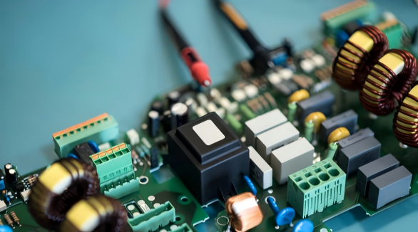
Explore critical creepage & clearance specifications for high voltage PCB design, including global standards and proven layout best practices.
2026/06/02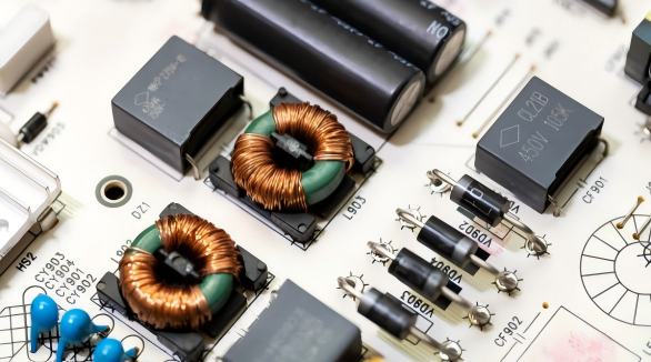
Learn PCB copper weight standards & balanced copper distribution rules to avoid warpage and boost board stability for electronic design.
2026/05/19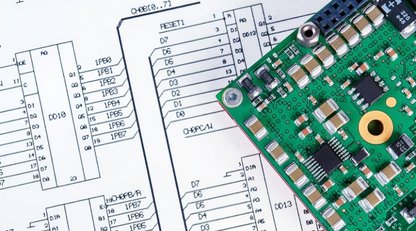
Learn common PCB design mistakes that cause assembly errors and follow DFM best practices to improve PCBA yield and reliability.
2026/05/14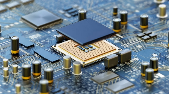
Learn professional copper pour techniques to boost PCB signal integrity, reduce EMI, improve thermal management, and ensure reliable manufacturing.
2026/04/16
Learn how to design mixed-signal PCBs with strong signal integrity using proven layout, grounding, and routing techniques for high-performance systems.
2026/04/09
Practical anti-ESD strategies for PCB design, including layer stack-up, layout, routing, component use and testing.
2026/04/02