- Products & Capabilities

- About
- Resources
PCBX.com Resources
Your source for industry knowledge, news, and expert insights

Latest Posts
Article
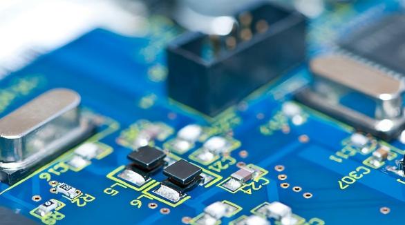
Learn practical PCB assembly methods to eliminate ground bounce & SSN, optimize signal integrity for high-speed electronics.
 2026/07/02
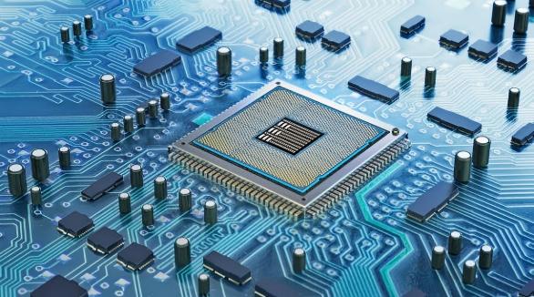
Compare FPGA and MCU core differences, PCB layout tradeoffs & use cases to select the best processor for your embedded hardware design.d
2026/06/30
Learn EMI, EMS & EMC definitions, differences and testing basics for electronic engineers in this EMC compatibility guide.
2026/06/25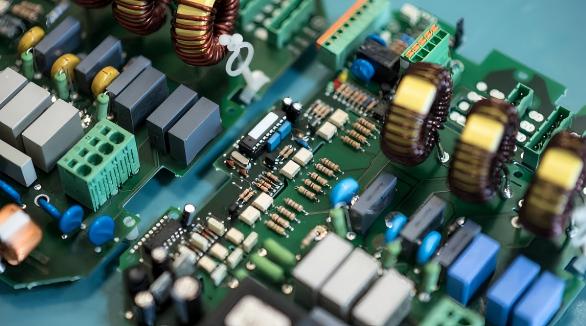
Learn proven PCB layout, grounding & stackup strategies to mitigate EMI, pass global EMC standards for high-speed electronics.
2026/06/23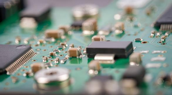
Learn how professional PCB enclosure design shields circuit boards from shock, moisture, EMI and overheating for reliable electronic hardware
2026/06/18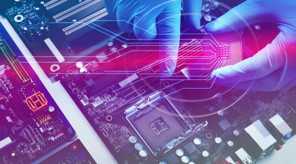
Learn full ECU PCB testing & validation workflows, core automotive standards, HIL verification, reliability solutions for EV & ADAS electronics
2026/06/16
Explore effective solutions to minimize PCB ringing via impedance matching, routing optimization, component selection and pre-production testing.
2026/06/11
Learn what PCB inner layers are, their types, functions, design rules, and common mistakes for reliable multilayer PCB design.
2026/06/09