
- Products & Capabilities

- About
- Resources
Root Causes Diagnosis and Practical Tips for Active Component Failures in PCBs


Diagnose PCB active‑component failures and explore root causes, test workflows & preventive tips for hardware and manufacturing engineers.
Printed Circuit Boards (PCBs) use active components like transistors, diodes, microcontrollers, power regulators and integrated circuits (ICs) to boost signals, control power and perform digital logic. These semiconductor devices require external power and have delicate internal structure and are the leading cause of circuit failure, production delays and permanent circuit board damage. For electronics technicians, design engineers and manufacturing quality teams, systematic troubleshooting of operating components failures optimizes repair processes and reduces damage to other hardware, especially when dealing with cascading component failures.
Primary Root Causes of Active Component Breakdown
Most active component failures are caused by 5 recurring stress factors which typically occur together to hasten degradation. Thermal overstress is the first one: The junction temperature of semiconductor devices is typically limited to 150°C; If there is insufficient copper heat plane, missing heat sinks, or prolonged overcurrent, then the junction temperature will exceed 150°C and cause the PN junction inside the semiconductor device to crack, resulting in permanent open circuit or short circuit. Another serious danger is electrical overload: A voltage spike, ESD and reverse bias damage the very small structure of the gates within an IC, and can create latently undetected defects. Vibration can cause mechanical wear which splits the solder joint or breaks the miniature SMD component lead, poor soldering can cause a solder joint to split or fail, and dust or water can cause a pin to corrode or cause leakage current. Manufacturing flaws including misaligned placement, incorrect reflow temperatures and mismatched component ratings also force semiconductors to operate outside safe specs and fail prematurely. Lastly, over the years of material aging, transistor gains fade and internal conductivity in ICs drift, causing a gradual deterioration in performance.
Standard Stepwise Troubleshooting Workflow
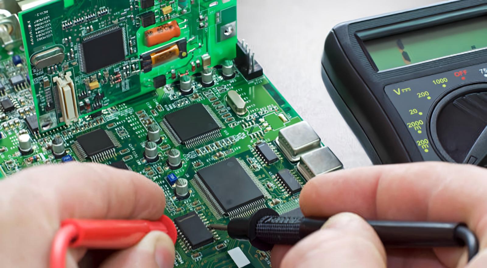
The approach used for diagnosis is non-destructive and multi-layered, eliminating secondary damage and concentrating on the best way to narrow down the fault. The process begins with a visual physical inspection of the parts, looking for black burn discoloration, chips bulging, cracked packages, cold solder joints and pin oxidation. This step will easily reveal apparent damage to the circuits by heat or assembly, and most minor defects will not be apparent, so the next step is electrical testing.
Baseline diagnostics are provided by power-off static testing using a multimeter. Technicians test diode forward voltage drops (0.6-0.7V for silicon diodes, 0.2-0.3V for Schottky diodes) and use the continuity check to find shorted regulators, and to check PN junctions of transistors. All readings should be checked to the official component datasheet to identify abnormal resistance or conduction. After static checks, the power-on dynamic testing stage measures clock, reset and communication bus waveforms on the MCUs and signal ICs with oscilloscopes, and searches for hotspots on the internal shorts in semiconductors under load with the infrared thermal cameras. When the fault is intermittent and ambiguous, circuit isolation and matched component replacement is used as final confirmation, and after a matched component is replaced, full PCB function is restored, and the failed part is confirmed as the fault source.
Targeted Diagnosis for Common Active Devices
The failure signatures and simplified test routines are different for each component category. In multimeter diode mode, transistors and MOSFETs will be detected as fully shorted pins or permanently open junctions; an additional test is provided for gate-source leakage in power MOSFETs. Diodes almost always fail as either a short or open and if it conducts in both directions, it is a burned rectifier; if it does not conduct, it has a shorted internal path. Complex ICs and microcontrollers require first the power pin voltage check, and if the clock signals are missing or distorted, then there is likely some damage to the internal chip, along with distorted register data and localized overheating. Power management ICs show obvious symptoms: No power output, large voltage ripple and high temperature at constant input power, indicating the failure of regulation circuits.
Essential Testing Tools & Advanced Diagnostic Tech
The three fundamental tools used for basic troubleshooting are the multimeters for static junction testing, oscilloscopes for real-time waveform analysis, and thermal imagers for non-contact hotspot detection. For advanced scenarios such as high-speed RF boards, dense multi-layer PCBs, additional equipment is required. LCR meters are able to detect small changes in impedance that are not detectable by multimeters, and thus detect early aging and parameter drift before system failure. In-circuit Testing (ICT) equipment tests the components without desoldering, which is perfect for mass production quality screening. High bandwidth oscilloscopes are used to measure signal integrity parameters such as jitter and overshoot to identify faulty high-speed switching ICs in digital circuits.
Avoiding Troubleshooting Pitfalls & Preventive Design Strategies
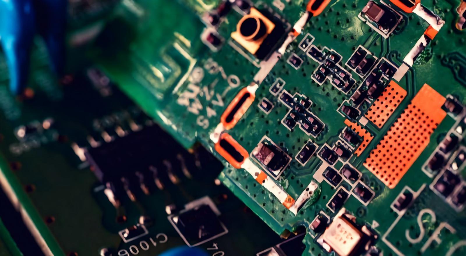
The three typical misjudgments that lose labor and harm PCBs: Swap a part that appears to be damaged when it is not, replace a part without verification, ignoring a peripheral passive circuit failure that can appear as if it is a failed active device. For reducing failures in the long-term, designers should use components whose voltage/current safety margins are at least 20% and incorporate ESD and surge protection circuits in the design, and optimize thermal layout of power semiconductors. Production teams need to ensure that their reflow soldering profiles are standardized and that the maintenance works, such as dust cleaning and thermal spot checking, are conducted periodically to replace the old parts ahead of time.
Troubleshooting active component failures is a mixture of circuit theory, practical instrument competence and systematic troubleshooting logic. Engineers can quickly identify the cause of root stress and limit equipment downtime by using the layering of inspection and testing steps, as well as diagnostic rules for each component. Regular board maintenance and preventive design further reduce failures and therefore extend the service life of electronic hardware in consumer, industrial and automotive applications. To ensure electronics developers worldwide can be confident that components will not fail in the field, PCBX is a specialist manufacturer of precision circuit boards with rigorous quality validation processes to minimize active component defects for reliable PCB prototyping, assembly and pre-production reliability testing.
Hot Tags:

Contact us

If you can't find what you're looking for, please contact us.
Article
Signal reflection in PCBs, due to impedance mismatches, can be managed with impedance matching, termination methods, and strategic layout to ensure reliability.
 2025/09/09
Analog signals are crucial in electronics but susceptible to noise, which necessitates strategic PCB design to ensure high performance and signal integrity.
2025/07/17
Routine inspections and proper maintenance of capacitors and resistors in PCBs reduce failures, prolong device lifespan, and lower maintenance costs.
2024/11/04