- Products & Capabilities

- About
- Resources
How to Reduce PCB Analog Signal Noise?


Analog signals are crucial in electronics but susceptible to noise, which necessitates strategic PCB design to ensure high performance and signal integrity.
Analog signals are the lifeblood of a wide range of electronic systems, from precision sensors to high-fidelity audio equipment. Analog signals are, however, notoriously vulnerable to noise interference that can dramatically affect performance and accuracy. With system performance hanging in the balance, designers must take careful steps to minimize noise in PCB analog circuits. This comprehensive guide examines the origins of analog signal noise and considers tried-and-tested strategies for achieving best-in-class signal integrity.
Understanding Analog Signal Noise
Analog signal noise is any unwanted electrical disturbance that degrades your desired signal. Unlike digital systems, which are very tolerant of distortion, analog circuits require extremely high signal purity in order to function correctly. Even low levels of noise can generate severe performance issues in the form of degraded signal-to-noise ratios, errors in measurement, communications errors, and limited dynamic range.
Chief Causes of Noise
Noise can be classified as both internal and external. The external causes of noise include radio frequency electromagnetic interference (EMI), power grid noise, and environmental noise. Internal noise comprises thermal noise, shot noise in semiconductor junctions, and power supply ripple. This complex array of noise sources demands a comprehensive approach to noise reduction.
Impact on System Performance
Noise contamination produces a number of significant effects:
Signal-to-Noise Ratio (SNR) Degradation: Reduces the system's ability to distinguish between useful signals and noise, directly affecting measurement accuracy.
Measurement Accuracy Loss: Particularly troublesome in sensor applications where signal changes provide important information; low noise can mask important information.
Communication Errors: Increases bit error rates and reduces effective transmission distance in analog communication systems.
Dynamic Range Limitations: Increases the noise floor, forcing designers to use higher signal levels or accept poorer performance.
Key PCB Layout Strategies
Strategic Partitioning of Circuits: Effective noise reduction begins with intelligent PCB layout that separates incompatible circuit functions. Put analog and digital circuits on opposite sides of the PCB. Utilize separate ground planes for analog and digital sections, connecting them together at a single star point near the power supply to prevent digital switching currents from affecting analog paths.
Trace Routing Optimization: Proper routing reduces susceptibility to noise by a great extent. Keep loop areas and trace lengths minimum. Use ground planes for providing short return paths for signals, and use orthogonal routing for minimizing crosstalk. For differential signals, maintain tight coupling and balanced trace lengths for maintaining balanced transmission.
Ground Plane Design Quality: Good ground plane design is critical to minimize noise. Provide solid ground cover under analog circuits and avoid breaks or slots that would force current detours. Utilize via stitching to connect ground planes on different layers, with minimum impedance and multiple return paths for high-frequency currents.
Power Supply Noise Mitigation
Advanced Decoupling Techniques: Decoupling of power supply in an efficient way requires a multi-dimensional filtering technique through the use of capacitors with different values. Utilize parallel combinations, for example, ceramic capacitors for high-frequency decoupling, tantalum capacitors for mid-range frequency, and electrolytic capacitors for low-frequency variation. Position decoupling capacitors close to IC power pins to minimize trace inductance.
Switching Regulator Optimization: When switching regulators are unavoidable for efficiency, employ frequency planning to avoid interfering with analog signals. Employ post-regulation filtering using linear post-regulators or LC filters to remove switching noise before it can interfere with analog circuits.
Advanced Grounding Strategies
Star Grounding: Utilize star grounding to prevent ground loops and noise circulation. All circuit grounds should be returned to one low-impedance point, typically near the main power supply. Keep high-current digital switching currents from sharing return paths with sensitive analog signals.
Ground Plane Architecture: Modern PCB designs rely on ground planes for power distribution and noise containment. Properly position ground planes in the PCB stack-up to provide shielding for signal layers and maintain controlled impedances. Use sufficient via counts to connect ground planes together, with priority given to high-current areas.
Filtering and Signal Conditioning
Passive Filter Design: Passive filters provide low-cost, easy noise filtering. RC and LC filters attenuate high-frequency noise quite well. Multi-stage filters using pi-section configurations can achieve very high levels of attenuation for stubborn noise issues.
Active Filter Solutions: Active filters using operational amplifiers allow greater design flexibility and can implement complicated frequency responses. Configurations like the Sallen-Key configuration provide good performance with general-purpose operational amplifiers.
Component Selection Guidelines
Low-Noise Semiconductors: Choose parts with more specification for gain-bandwidth products and noise density. Provide for input bias current requirements for high-impedance sources.
Passive Components: Employ metal film resistors for lower noise than carbon composition resistors, and capacitors that provide high-frequency performance with stability sufficient for the application.
Shielding and Protection Methods
Internal Shielding: Use PCB-mounted shield cans over sensitive analog circuits and establish compartments in enclosures to separate analog and digital sections.
Cable Management: Route sensitive analog cables away from noisy digital cables and power conductors. Use grounded cable shields and good filtering at connective points.
Testing and Validation
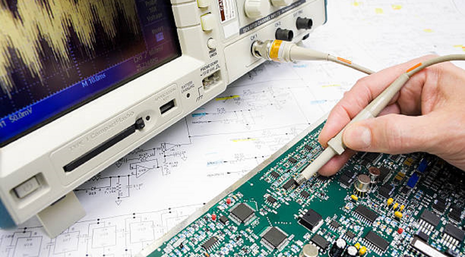
Noise reduction is an iterative process, and measurement and verification should be performed with severity. Utilize oscilloscopes with appropriate bandwidth and sensitivity, and utilize spectrum analyzers to quantify noise levels in the frequency domain. Conduct environmental testing to ensure real-world performance satisfies design requirements.
Achieving low-noise analog signal performance in PCB design is a scientific process that entails optimization of the layout, judicious selection of components, and full power supply design. Realizing the inherent complexity of noise sources and solving them simultaneously ensures effective noise reduction. By following these strategies, engineers can achieve the clean, precise analog signals that high-performance electronic systems demand. With careful measurement and verification at each step along the way, even the most difficult applications can achieve excellent noise performance, preserving signal integrity and system reliability.
Hot Tags:

Contact us

If you can't find what you're looking for, please contact us.
Article
eFuses are advanced PCB fuses that reset automatically, offering fast, precise protection and versatility in electronics, enhancing device safety and reliability.
 2024/11/12
PCB short circuits arise from unintended connections, leading to safety risks. Prevention involves isolation, inspections, and thermal protection, ensuring device reliability and safety.
2024/10/23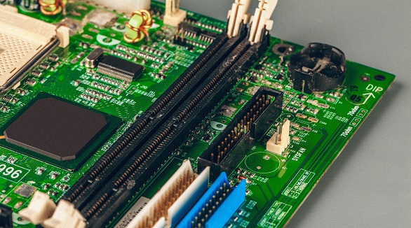
Efficient PCB assembly needs component standardization, design clarity, optimized workflow, material management, defect detection, automation, teamwork, lean practices, and IoT integration to meet quality and demand.
2024/10/21