- Products & Capabilities

- About
- Resources
How to Avoid Signal Reflection in PCB Design?


Signal reflection in PCBs, due to impedance mismatches, can be managed with impedance matching, termination methods, and strategic layout to ensure reliability.
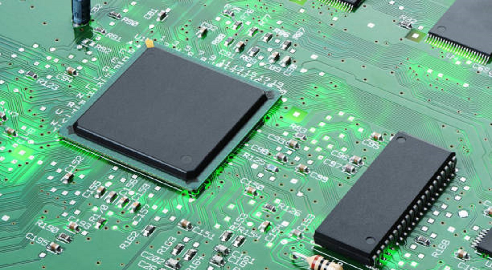
In the high-speed world of electronics, printed circuit boards (PCBs) are the foundation for nearly everything from a basic gadget to a sophisticated computer system. Signal integrity is one of the significant concepts in PCB design, referring to the fidelity and character of electrical signals on the board. In high-speed applications, minor distortions or signal loss can significantly compromise performance. Among the danger of signal integrity is signal reflection, which leads to data transmission interference and system unreliability. This article discusses the cause and impact of signal reflection as well as practical solutions to combat its influence in PCB design.
Signal Reflection
Signal reflection occurs when a signal that travels meets an impedance discontinuity along its journey, for example, when a PCB trace is incompatible with the source or load impedance. This impedance mismatch leads to a portion of the signal being reflected back towards the source, just like waves rebounding off a surface or a ball bouncing back off a wall. If not handled, signal reflection can lead to signal distortion, corruption of data, and overall system instability that poses a serious challenge in the realization of the intended electronic component performance.
Causes of Signal Reflection
Impedance Mismatch: Impedance mismatch, one of the leading causes of reflection, is when trace impedance is not compatible with the source or load impedance. The mismatches may be caused by variations in trace width, inconsistencies in the dielectric material, or inefficient termination practices.
Transmission Line Effects: PCB traces exhibit transmission line characteristics at high frequencies. If they are not well designed and applied, they have the tendency to make signal reflections unnecessarily complex, particularly in high-speed designs.
Interference and Crosstalk: Signal reflections do have the potential to interfere with the original transmission, leading to distortion and corruption of data. The issue is aggravated if there is crosstalk between traces, as this produces more noise as well as more system instability.
The Impact of Signal Reflection
Signal reflection can have some adverse effects on PCB performance:
Signal Distortion: Added reflected signals to the original transmission can cause overshoot, undershoot, and ringing. Distortion can disturb proper signal interpretation.
Data Corruption: Distorted signals can corrupt data transmission, causing system compromise on reliability and performance.
System Instability: Reflection of the signal leads to unpredictable voltage levels or noise, which can cause intermittent failure, glitches, or even system crashes. This kind of instability is particularly disconcerting in high-reliability situations, such as medical devices and spacecraft systems.
Avoiding Signal Reflection: Effective Techniques
In order to make PCB performance dependable, it's important to prevent signal reflection by careful design techniques. Some practical solutions are as follows:
Impedance Matching
Achieving impedance matching is crucial to prevent reflection in signals. Trace impedance when matched with load and source reduces the likelihood of reflection.
Trace Impedance Calculation: Use online calculators or high-end software like Altium Designer to calculate the correct impedance by inputting trace dimensions, PCB stack-up information, and dielectric properties.
Tuning Trace Parameters: Alter such parameters as trace width, trace spacing, and dielectric material to modify impedance. Wider traces and narrower spacing will form lower impedance, and narrower traces and greater spacing raise impedance.
Termination Methods
Efficient termination arrests reflected power and places impedance in the correct relationship, reducing the chance of signal reflection.
Series Termination: Connects a resistor in series with the signal source, suitable for point-to-point uses where the load impedance is high.
Parallel Termination: Places a resistor between the signal line and ground at the load end, effectively consuming reflections at the load point.
Thevenin Termination: Utilizes resistors together to match impedance and provide a steady voltage level, commonly used in systems that require precise voltage regulation.
PCB Layout Guidelines
Using the following strategic layout practices can significantly reduce signal reflection likelihood and impact.
Control Trace Lengths: Keep trace lengths as short as possible to minimize signal degradation and possible issues with reflections. Shorter length traces minimize the possibility of timing problems and maintain signal integrity.
Avoid Sharp Bends: Rather than using sharp 90-degree bends, use soft curvatures or 45-degree angles to avoid impedance discontinuities that lead to reflections.
Use Differential Signal Routing: Drive high-speed signals as differential pairs with precise spacing to fight noise and keep signals intact. Differential pairs cancel potential interference, resulting in better overall signal quality.
Correct Component Placement: Place components so that it reduces trace length and does not cross signal path lines. Short and straight connections reduce reflections and crosstalk, leading to better performance.
Via Considerations to Use
Vias between different layers on a PCB create impedance discontinuities.
Limit Via Usage: Do not place unnecessary vias in signal traces to provide stable impedance.
Back-drilling and Blind/Buried Vias: Use back-drilling or use blind/buried vias to reduce the effect of via stubs, leading to reflections in high-speed designs.
Effective bypassing of signal reflection is required to optimize PCB design and provide stable signal integrity, particularly in high-speed design. By understanding signal reflection mechanisms and using focused methods such as impedance matching, effective termination, and thoughtful layout design, engineers are able to effectively reduce the adverse effects of reflection. These methods not only enhance the performance of PCBs but also their stability and reliability during use. As electronic designs become more sophisticated, keeping up with these skills is crucial for attaining peak circuit performance, guaranteeing that devices operate dependably in ever-increasing demanding conditions.
Hot Tags:

Contact us

If you can't find what you're looking for, please contact us.
Article

Capacitors are crucial in PCB design for filtering and timing. Correct polarity in electrolytic and tantalum types prevents malfunctions and ensures reliability.
 2025/01/09
eFuses are advanced PCB fuses that reset automatically, offering fast, precise protection and versatility in electronics, enhancing device safety and reliability.
2024/11/12
High-speed PCBs (>1GHz) are crucial for advanced electronics like 5G and data processors. Key practices include ensuring signal integrity, controlling EMI, and maintaining power integrity for reliable performance.
2024/09/27