
- Products & Capabilities

- About
- Resources
Analog vs. Digital Ground: A Practical Guide to Mixed-Signal PCB Layout


Learn how to manage analog and digital ground in mixed-signal PCB layout to reduce noise and improve signal integrity.
Ground is frequently treated as an afterthought during schematic capture, a single net that ties every reference point to zero volts. In practice, ground is one of the most consequential decisions an engineer makes, particularly on boards that combine sensitive analog circuitry with fast digital switching. Mixed-signal PCBs, common in instrumentation, sensor interfaces, motor control, and automated test equipment, depend heavily on how well the designer manages the interaction between analog and digital return currents. A board that mismanages this interaction does not always fail outright; more often it works on the bench but exhibits noise, offset drift, or intermittent measurement error that is difficult to trace back to its source.
Why Analog and Digital Ground Behave Differently
The distinction between analog and digital ground is not a matter of voltage level, since both are nominally at zero volts. The distinction lies in the character of the current each path carries. Digital ground supports circuitry that switches current in short, high-slew-rate pulses as logic gates transition and capacitive loads charge and discharge, generating broadband noise at each edge. Analog ground supports circuitry that must preserve a continuous, low-level signal without distortion, such as sensor front ends, precision amplifiers, or the reference path feeding an analog-to-digital converter. Both ground types function as low-impedance copper planes that give return currents a defined path and serve as a stable reference for the signals routed above them, but the demands placed on that reference differ sharply between the two domains.
The underlying problem is shared impedance. No real ground plane has zero impedance. When switching current from digital circuitry flows through a path also shared by an analog return current, the digital transient induces a voltage drop across that shared impedance. This voltage appears as noise superimposed on the analog reference and couples directly into the measurement chain, since analog circuits are almost always referenced to ground. The severity of this coupling scales with the switching current's magnitude, its rate of change, and the impedance of the shared path, which is why the problem intensifies as digital clock speeds and edge rates increase. A related effect, sometimes called ground bounce, occurs when a rapid current draw interacts with the parasitic inductance of a trace or plane, producing a momentary voltage wobble that can propagate into nearby sensitive nodes.
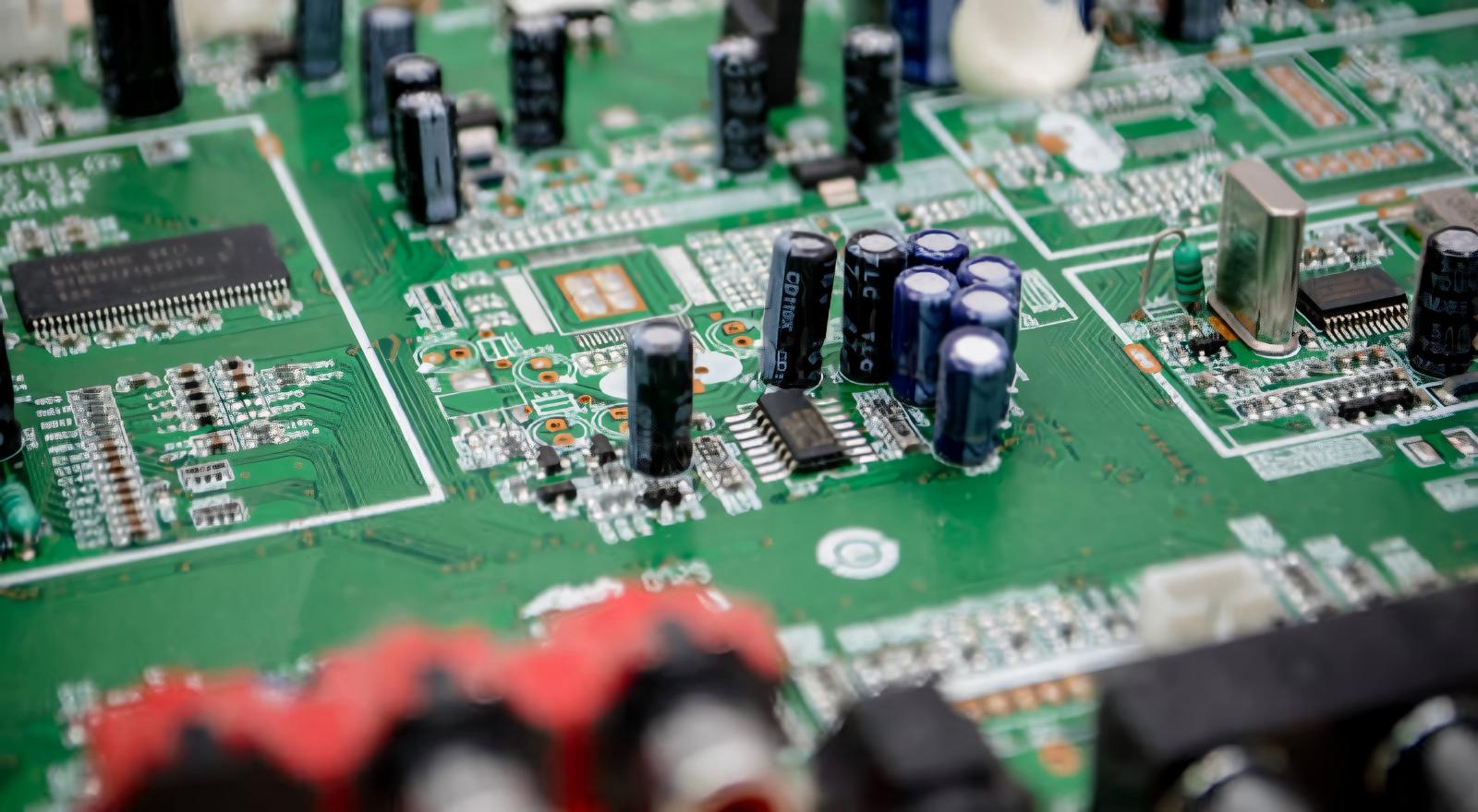
Split-Plane Versus Solid-Plane Strategies
Conventional guidance for many years called for physically splitting the ground plane into separate analog and digital regions, joined at a single point near the mixed-signal device. This approach can be effective, but it is easy to apply incorrectly. A split only helps if every trace crossing between the two domains has a return path routed directly beneath it; a trace crossing the gap without that support forces its return current into a long detour around the split. That detour enlarges the current loop, which increases both radiated emissions and susceptibility to external noise, often producing a worse outcome than an unsplit plane would have.
For most modern mixed-signal designs, a single continuous ground plane combined with disciplined component placement is the more reliable strategy. Digital devices, their decoupling capacitors, and any switching regulators are grouped together so that high-current return activity stays confined to one region of the board. Analog devices occupy a separate region with short, direct return paths. The point where the two domains meet, typically at a data converter, is handled with attention to how the device's analog and digital pins actually connect to the copper beneath the package. This approach relies on geometry and placement rather than a plane discontinuity, avoiding the return-path hazards a poorly executed split can introduce.
Practical Layout Practices
A number of practices consistently improve mixed-signal ground performance regardless of which topology is used. Component placement should minimize the distance that digital return current must travel, keeping regulators, oscillators, and digital I/O away from sensitive analog input stages. Sensitive analog traces should avoid running directly above or beside digital traces on an adjacent layer, since this creates coupling paths that a solid ground plane alone cannot fully suppress.
Decoupling capacitor placement is equally important. Each active device benefits from local decoupling capacitors placed close to its supply pins, connected to ground through a short, low-inductance via. Local decoupling means high-frequency current is supplied close to the device rather than pulled across the board, limiting the noise injected into the surrounding ground structure. Star-point grounding for power returns, distinct from signal ground topology, is worth considering in systems with multiple supply rails, since bringing high-current returns to a single point near the source prevents supply ripple from modulating the analog reference elsewhere on the board.
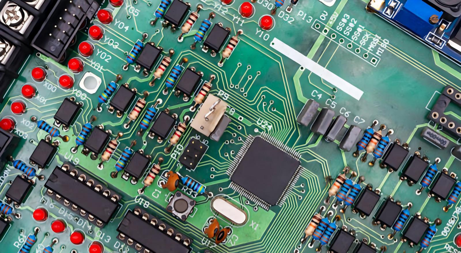
Layer stack-up is another factor that is easy to underestimate. A four-layer or six-layer stack with an uninterrupted ground plane directly adjacent to the signal layers gives every trace a low-impedance return path immediately beneath it, often achieving better noise control than any amount of net separation on a two-layer board. Where layer count and budget allow, dedicating a full layer to ground and positioning it next to the layer carrying the most sensitive analog traces is one of the highest-leverage decisions available during stack-up planning.
Ground Strategy as a System-Level Decision
Managing analog and digital ground cannot be resolved by a single rule applied uniformly across a layout. It requires understanding where switching currents originate, how far they travel, and which nodes are most exposed to the resulting noise. Engineers who treat grounding as a system-level question early in the design process, rather than a net-assignment task left until the end of layout, consistently produce mixed-signal boards with lower noise floors and more repeatable measurement performance.
For manufacturers producing mixed-signal boards across varied industrial, life sciences, and test equipment applications, these grounding decisions are also DFM considerations that influence first-pass yield and functional test outcomes, which is why PCBX's engineering review process pays particular attention to ground plane continuity and analog/digital partitioning before a design moves into fabrication.
Hot Tags:

Contact us

If you can't find what you're looking for, please contact us.
Article
Learn how to design mixed-signal PCBs with strong signal integrity using proven layout, grounding, and routing techniques for high-performance systems.
 2026/04/09
Optimize PCB layout for manufacturability by ensuring proper trace clearance, via placement, and incorporating testability features, while considering manufacturing tolerances.
2025/07/03
Power and ground planes in PCBs ensure signal integrity, manage heat, and minimize EMI, crucial for efficient, high-performance electronic devices.
2024/11/11