- Products & Capabilities

- About
- Resources
Common Mistakes to Avoid in PCB Layout


Optimize PCB layout for manufacturability by ensuring proper trace clearance, via placement, and incorporating testability features, while considering manufacturing tolerances.
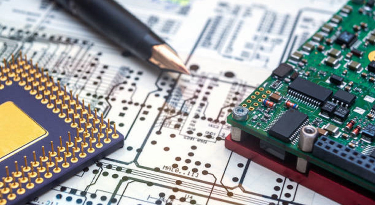
PCB layout design is a product design foundation that has a significant influence on the end product's manufacturability, performance, and reliability. Replication of typical design errors can result in more expensive production, increased lead times, and reduced product functionality.
Role of Manufacturability in PCB Layout Design
A PCB's layout design has a crucial role in its manufacturability. A carefully planned design layout not only assures the correct operation of the circuit, but also efficient and cost-effective production. Inefficiently designed layouts, on the contrary, lead to a series of manufacturing problems, such as an increased rate of scrap, loss of yield, and an increased overall cost. The realization and prevention of these design pitfalls allow PCB designers to better plan their designs for today's manufacturing process and provide high-quality product on time and at budget.
Common PCB Layout Design Errors to Avoid
Trace and Space Clearance that is too low
Trace and space clearance is the amount of space between two adjacent copper traces and between a trace or pad, and it is most important to avoid shorts and electrical leakage. Inadequate clearance will lead to a multitude of manufacturing defects, including shorts, electrical leakage, and etching and plating distress. With inadequate clearance, the solder mask application process is not advisable, and solder bridges and assembly-related issues are induced.
Tip: Always maintain minimum trace and space clearance requirements as set by your PCB manufacturer or utilize industry standards like IPC-2221. This practice will yield manufacturability and reliability with due care.
Poor Via Placement and Design
Vias are key elements that connect alternate copper layers of a PCB. Inaccurate placement or design of vias can make the drilling and plating processes tedious, affect structural integrity, and even lead to impedance mismatches.
Tip: Be sure to keep a close eye on the manufacturer's via design guidelines, noting via diameter, aspect ratio, and placement strategy. This guarantees solid connectivity between layers and reduces performance issues.
Insufficient Copper Weight and Trace Width
Copper weight and trace width are significant in manufacturability, electrical performance, and thermal management of the PCB. Failure to consider these will result in etching and plating issues, leading to defects and lower yields. Thermal management issues also hinder the PCB from dissipating heat, which affects performance.
Tip: Use manufacturers and industry standards to select the appropriate copper weight and trace widths based on factors like current-carrying ability and thermal management needs.
Insufficient Solder Mask Clearance
Solder mask is a critical function that protects copper traces and prevents shorts on assembly. Insufficient solder mask clearance will result in solder bridges, shorts, and solder mask application hindrance, resulting in defects and reduced yields.
Tip: Follow solder mask clearance guidelines from the PCB vendor or specified in those standards like IPC-2221. This is to prevent solder issues, and the board becomes more dependable.
Poor Silkscreen Placement and Layout
Silkscreen layer has component designators, logos, and other marks that are important to assembly and diagnosis. Poor placement can lead to assembly interference and lower readability, resulting in assembly errors and cosmetic defects.
Tip: Provide careful silkscreen design such that it is readable and relevant but does not get in the way of component placement. This will enhance useability and aesthetics of the PCB.
Disregard of Manufacturing Tolerances
Every manufacturing process has a tolerance. Disregarding these results in losses in yield, reliability issues, and increased expense in non-conforming boards and tighter restrictions enforced in design.
Tip: Communicate with the manufacturers to understand their tolerances and incorporate these factors into your design. This step will yield efficient production and high-performance products.
Lack of Considering Test and Inspection Processes
Lack of considering test and inspection processes leads to test difficulty, inspection issues, and undetected flaws that influence reliability.
Tip: Work with your manufacturing firm to establish their inspection and test needs. Build in design elements that allow for these functions, with careful quality assurance.
Component Placement and Orientation Neglect
Component placement plays an extremely high impact on manufacturability and assembly efficiency. Incorrect placement can create assembly problems, interfere with other components, and create thermal problems.
Tip: Place components for best fit according to size, heat generation, and type of assembly. Allow interference prevention by proper spacing, especially for heat-generating components.
Failure to Use Design for Testability (DFT)
Design for Testability (DFT) allows the PCB to be more easily tested during manufacture. Failure to implement DFT concepts can make testing harder, increase debugging time, and decrease fault coverage.
Tip: Incorporate DFT into the design by adding test points, self-test capability, and other testability features. This improves the effectiveness of quality assurance processes.
Disregard for Manufacturing Processes and Equipment Capabilities
Each PCB manufacturing facility has its processes, equipment, and capabilities. Disregarding them leads to incompatibility, increased lead times, and higher cost.
Tip: Have early discussions with your PCB fabricator to know their individual process capabilities. Design keeping these capabilities in mind to ascertain compatibility and affordability.

Proper PCB design layout is intricate, requiring careful attention to detail and the utmost knowledge of varying design considerations. Steer clear of these traps and the use of best practices, designers in PCBX provide a minimum manufacturability and performance, and allow reliability and efficiency in the current manufacturing process. Regular liaison with manufacturers and staying updated with design principles and industry standards helps to remain competitive in the line of work.
Hot Tags:

Contact us

If you can't find what you're looking for, please contact us.
Article
PCB schematics map circuit connections, while layouts focus on physical design for manufacturing. Both stages ensure optimal and reliable PCB design.
 2025/02/11
DFM ensures cost-effective PCB design by optimizing size, layers, materials, and components, focusing on manufacturability, reliability, and process efficiency.
2024/10/30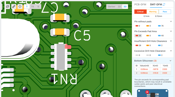
The article is developed concerning the breakthrough of integrated circuits and the need for custom PCBs in some electronic products. It enumerates ten golden rules in conducting PCB layout design and manufacturing: grid selection, routing, power layers, component placement, panel duplication, component value combination, frequent DRC, flexible silkscreen use, decoupling capacitors, and pre-production parameter checks. These rules provide for the optimum design and manufacturing of a PCB.
2024/07/25