- Products & Capabilities

- About
- Resources
Designing Mixed-Signal PCBs for Optimal Signal Integrity


Learn how to design mixed-signal PCBs with strong signal integrity using proven layout, grounding, and routing techniques for high-performance systems.
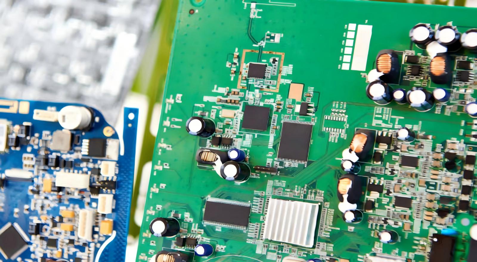
A mixed-signal PCB needs to be carefully designed to coordinate without compromising analog precision or digital speed. As these two domains are highly different, inadequate design decisions can readily inject noise, distortion, and electromagnetic interference (EMI). It is not necessary to use isolated techniques to achieve high signal integrity, but a combination of layout, grounding, routing, and power design strategies should be viewed as a single design approach.
Start with Functional Partitioning
The initial and the most important is the clear division of analog and digital.
The analog circuits, e.g. amplifiers and data converters, are very sensitive to noise and digital circuits produce switching noise because of rapid transition. To minimize interference:
Install analog and digital parts in different areas of PCB
Locate ADC and DAC parts at interface
Arrange elements in signal flow direction, without superfluous crossings
This well-organized structure separates noise coupling prior to routing even starting and makes the whole design process easier.
Design an Effective Grounding System
Signal integrity is primarily based on grounding. No other factor can cause more problems than a poorly designed ground.
A continuous ground plane is usually desirable, as opposed to split planes, since it offers all signals a low-impedance path back to ground. Key practices include:
Ensuring that the return currents are flowing under the respective signal traces.
It is not advisable to route over splits or gaps in the ground plane.
Linking analog and digital grounds to a common reference point which is under control in case segregation is required.
It is necessary to understand the behavior of the return current. High-frequency signals will take the route of minimal impedance rather than the minimal distance, and therefore it is important to ensure continuous ground planes.
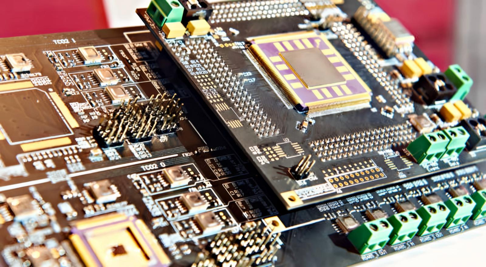
Stack-Up Optimization Signal Integrity
Proper PCB stack-up enhances not only electrical but also noise performance.
Signal layers should be placed near solid ground planes to ensure that the impedance is controlled.
Isolate noisy and sensitive signals with a multilayer structure.
Mutually perpendicular so as to minimize crosstalk.
As an example, a standard four-layer stack could be composed of top and bottom signal layers with an inner ground and power plane. This design offers shielding and fixed reference planes, which are vital in high-speed designs.
Control Distribution of Power
Signal integrity is directly related to power integrity. Both analog and digital circuits may be affected by noise on power rails.
To deliver clean power:
Apply different or filtered power to analog and digital sections.
Install decoupling C near each IC power pin.
Add several values of capacitors to span a large frequency range.
Keep loop areas to a minimum between power and ground to minimize inductance.
Adequate power distribution can keep the voltage levels constant and does not allow the noise to propagate throughout the board.
Use Disciplined Routing Techniques
The practice of routing involves the theory and practice coming together. All design efforts may be undone by poor routing.
Digital signals:
Ensure low controlled impedance of high-speed traces.
Keep tracks short and straight.
Stubs, sharp bends and unnecessary vias should be avoided.
Analog signals:
Divert them off digital switching indications.
Do not use long parallel routing that is with noisy traces.
Guard sensitive lines with guard traces or ground shielding.
Also, the correct separation between tracks can minimize crosstalk and differentiating signals can enhance noise resilience in critical paths.
Eliminate Noise and EMI Sources
Noise management is an issue that is taken into consideration during the design.
Isolate high-speed lines and clock signals, which are important sources of noise.
Minimize clock traces and do not route them close to analog areas.
Shielding through use with stitching and ground fills.
Keeping loop areas as small as possible to reduce radiated emissions.
These methods will aid in avoiding both radiated and conducted interference, thus guaranteeing a stable system performance.
Pay Attention to Return Paths
All signals shall have a distinct and unbroken return path. Lack of consideration of this principle usually results in some noise problems.
Make sure that signal traces can be passed over by direct currents.
Do not run signals over plane breaks or coplanar interfaces.
Give neighboring ground vias where changing layers to ensure continuity.
An effectively controlled return path minimizes loop inductance and assists in preserving signal integrity throughout the board.
Check by Simulation and Test
Even professional designers use validation tools to guarantee performance.
Simulate signal integrity to examine reflections and impedance.
Assess risks of crosstalk and EMI pre-fabrication.
Perform prototyping, functional, and electrical testing.
The use of simulation and testing gives the assurance that the design will work in the real world and in a dependable manner.
The process of designing a mixed signal PCB with a high signal integrity demands a whole board view that integrates partitioning, grounding, stack-up planning, power management, and prudent routing. Successful designs are not trying to treat these elements independently but rather combine them into some kind of a unified approach to reducing noise and ensuring clean signal paths.
Mixed-signal systems grow more complex and faster and adherence to these principles is all the more significant. PCBX provides wide-ranging solutions that assist in optimization of signal integrity and assures high-performance PCB results throughout the design to the production.
Hot Tags:

Contact us

If you can't find what you're looking for, please contact us.
Article
PCB failures due to minor orientation and polarity errors can impact reliability, but proper design practices and checks ensure manufacturability and performance.
 2025/12/18
Signal reflection in PCBs, due to impedance mismatches, can be managed with impedance matching, termination methods, and strategic layout to ensure reliability.
2025/09/09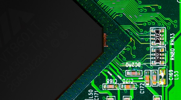
Tab routing enhances PCB production efficiency and quality, ideal for complex shapes. It offers cost-effectiveness, flexibility, and protection, crucial for high-precision designs and panelization.
2024/10/23