PCBX.com Resources
Your source for industry knowledge, news, and expert insights

Latest Posts
Article

Signal reflection and distortion, resulting from impedance mismatches, impact PCB performance and require strategic design, simulation, and material selection for mitigation.

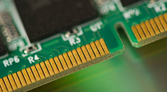
Edge connector bevelling enhances PCB durability and reliable connections, vital for frequent usage and secure engagements, with limitations primarily in plating.

FR4 permittivity affects PCB signal speed and impedance. It's crucial for design, requiring careful management in high-frequency applications for reliability.

Schematic diagrams use standardized symbols to illustrate electronic circuits, essential for design, analysis, and construction, bridging concepts and reality.

Tab routing in PCB manufacturing boosts efficiency and quality, ideal for non-linear shapes, offering flexibility, support, and cost-effectiveness in production.

Tab routing enhances PCB production efficiency and quality, ideal for complex shapes. It offers cost-effectiveness, flexibility, and protection, crucial for high-precision designs and panelization.

PCB design trends include miniaturization, advanced materials, sustainability, automation, and security, aligning with technological advances and diverse industry demands.

Designing PCBs for IoT demands innovation to tackle space, power, connectivity, and security challenges, ensuring robust, efficient, cost-effective devices that meet modern technological demands.