- Products & Capabilities

- About
- Resources
Challenges and Strategies in IoT PCB Design


Designing PCBs for IoT demands innovation to tackle space, power, connectivity, and security challenges, ensuring robust, efficient, cost-effective devices that meet modern technological demands.
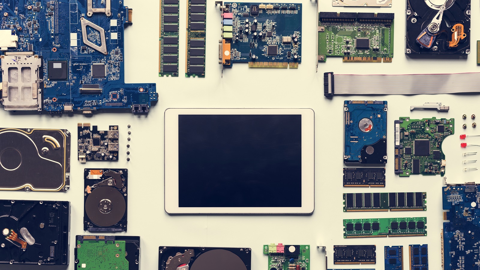
PCB design for IoT products becomes a rather daunting and intricate task that requires innovation with a farsighted approach. From smart home devices to industrial sensors, IoT is seriously redefining the way we interact with technology by packing advanced features into compact dimensions. At the very core of such devices, PCBs facilitate functionality and connectivity. Key challenges and their strategic solutions while preparing PCB designs compatible with the requirements of IoT applications: space-efficient, cost-effective balance with performance.
Introduction: The Essential Role of PCBs in IoT
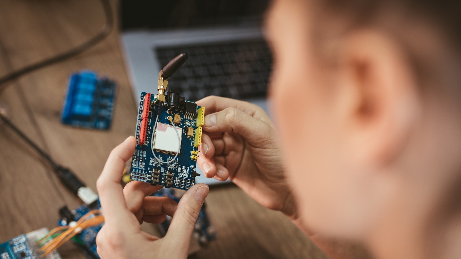
The IoT happens to be one of the most important technological evolutions that embeds connectivity into diverse device forms across several industries. In this transformation, a vital role is played by Printed Circuit Boards, or PCBs. They are the physical interfaces for sensors, processors, and communication modules. With the expansion in the reach of IoT, efficient PCB design becomes quite essential to ensure that different devices play their roles efficiently and sustainably. Such designers need to overcome a variety of challenges related to compact size, power efficiency, connectivity, and security-all defining the functionality and reliability of IoT devices.
Miniaturization and Space Constraints
One of the main challenges in IoT PCB design is this drive for smaller yet more powerful devices. Users are asking for devices that will befit the surroundings with a minimum loss of power or functionality, which forces extraordinary innovation from the engineers.
HDI technology, or High-Density Interconnect, becomes necessary to achieve miniaturization. Finer lines and smaller vias are used to accommodate more components within scant space. Complementing this is SoC technology, adopted to integrate more functionalities on a single chip, hence reducing the discrete components needed. Moreover, the use of multilayer PCBs with circuits stacked vertically enhances complexity handling and allows more features within a confined footprint. These strategies together ensure that devices can meet both aesthetic and functional modern expectations without compensating on reliability.
Power Management
Effective power management is crucial since many IoT devices are dependent on batteries and/or alternate means of energy harvesting for continued operation. The challenge is in prolonging battery life without compromising performance.
These challenges can be addressed through the use of components that are explicitly designed to consume very low power, so as to extend the runtime of the device tremendously. For instance, the utilization of sleep modes and duty cycling enables the device to draw minimum energy when not active, without affecting crucial functionalities. The power of the device is supplemented through the use of harvested energy-solar power or kinetic-to-electrical energy conversion-particularly when devices are operational in off-grid, remote locations. This approach will further increase the autonomy of the device and be in accord with sustainability objectives by minimizing reliance on conventional sources of power.
Connectivity and Communication Protocols
The ability of devices to communicate fluently across a wide variety of platforms and networks is one of the main characteristics of IoT. This in turn requires solid multi-protocol support for Bluetooth, Wi-Fi, and Zigbee, among others.
Optimized antenna design and placement will be able to sustain strong and reliable connectivity, crucial for fluent data exchange. Integration of printed or integrated antennas within the PCB will optimize space while allowing performance. They also develop general and flexible PCBs that support multiple and sometimes changing protocols in order to keep the devices relevant within the changing technological environment. Appropriate shielding and grounding practices are employed to reduce EMI issues and keep data intact and communication clear. All put together, these strategies ensure that IoT devices can interact robustly and effectively in complex networked environments.
Signal Integrity and EMI Management
IoE devices need signal integrity to be maintained in high-frequency, extremely dense environments for reliable operations. Poor signal integrity will greatly deteriorate performance and even cause EMI.
Impedance matching techniques are implemented to keep trace routing in check, ensuring the lowest possible signal reflections for high-integrity data. Incorporation of dedicated power and ground planes further isolates the signals and reduces interference risks to ensure circuit reliability. Also, the addition of filtering components such as capacitors and inductors helps keep voltage levels stable and minimizes the impact caused by transient disturbances. Such strategies necessarily go with optimizing performance and making the IoT device resilient enough for reliable operations under a wide variety of contexts and conditions.
Thermal Management
The Internet of Things devices normally have a low power consumption, but they generate a lot of heat due to high circuit density and processing requirements. Therefore, thermal management is very important in the avoidance of overheating, which can actually destroy it and affect its stability over time.
Overcoming thermal challenges includes the consideration of designers in the effective use of vias and heat-conductive materials that can help dissipate heat from critical components. Simulation tools used early in the design process assist in making realistic predictions and take active control of potential thermal issues by optimizing layouts for better heat distribution. Further thermal management, without increased size, is provided by designing device enclosures to serve as passive heat sinks. All these strategies together ensure that IoT devices will perform well and be reliable in a wide range of operational environments.
Security and Data Privacy
With IoT devices having to process and at times store larger volumes of sensitive data over wider networks, their security and the privacy of data are of utmost importance. Strong confidence in security measures, deeply embedded in printed circuit board designs, acts to protect against unauthorized access and breaches.
The use of hardware-based encryption methods in conjunction with secure boot processes alone guarantees integrity for both data storage and transmission. Besides, integration of tamper-detection capabilities will add to the physical security to serve in the notification of users on attempts of unauthorized access. Such embedded capabilities in IoT devices will help ensure protection to user information and trust in deployed networks to enable further connected technologies adoption.
Cost-Effectiveness
The IoT market is very competitive, and cost-effective design solutions alone can make such products more affordable without any compromise in quality or functionality.
The principle of DfM drives the manufacturing of the PCBs by utilizing only standard components and efficient ways of assembling the boards. This reduces costs, while early prototyping allows the early detection and fixing of design issues, hence reducing the number of potential late-stage production errors or faults that may be encountered at a higher cost. Besides, good relationships with suppliers provide competitively priced components and will further assist in containing costs. All in all, these various approaches balance affordability with performance, thereby enhancing the competitiveness of IoT technologies and their accessibility.
Conclusion: Balancing Complexity with Functionality
The IoT application-based PCB design involves complex issues on various dimensions, which require similarly sophisticated engineering solutions. With major focuses on miniaturization, power efficiency, connectivity, security, and cost, one is able to develop robust devices that are efficient in performance and adaptability according to rigorous demands in the modern world. Advanced PCB design has to be increasingly important as IoT technologies are continuously evolving and finding their use across a wide array of industries, opening up new uses and further innovations that would greatly improve connectivity and redefine industries worldwide. Strong design processes by engineers empower this new wave of IoT devices that spur advancements and make lives better through seamlessly integrating smart technology into daily environments.
Hot Tags:

Contact us

If you can't find what you're looking for, please contact us.
Article
Solder masks protect PCBs from environmental damage and electrical shorts, enhancing reliability and aesthetics. The application is complex, requiring professional fabrication to ensure quality and compliance with regulations.
 2024/08/20
The article is developed concerning the breakthrough of integrated circuits and the need for custom PCBs in some electronic products. It enumerates ten golden rules in conducting PCB layout design and manufacturing: grid selection, routing, power layers, component placement, panel duplication, component value combination, frequent DRC, flexible silkscreen use, decoupling capacitors, and pre-production parameter checks. These rules provide for the optimum design and manufacturing of a PCB.
2024/07/25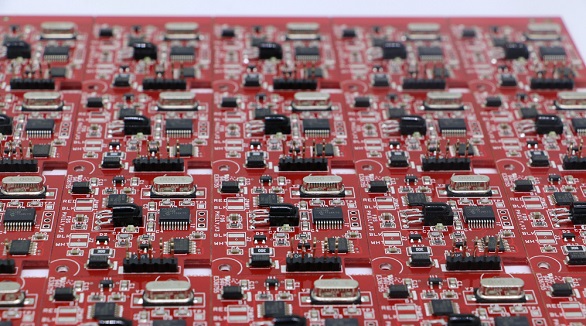
Thermal management is all about more than just keeping the temperature of electronic systems and printed circuit boards low. It has been a key issue related to reliability and performance. Of the very basic fundamentals that would be studied in the field, some are concerned with methods of heat transfer. These are through conduction, convection, and radiation. The methods of cooling include natural cooling, forced-air cooling, fluid cooling, and evaporation cooling. Appropriate thermal design rules shall be followed wherein the chosen materials provide optimum thermal conductivity and the components of a system are so laid out that no hot-spotting will take place. Thermal analysis becomes critical in pointing out heat-related issues and optimizing the design. It thus minimizes failure rates and enhances stability and functionality of the electronic systems through comprehensive thermal management.
2024/07/25