- Products & Capabilities

- About
- Resources
PCBX.com Resources
Your source for industry knowledge, news, and expert insights

Latest Posts
Article

Explore effective solutions to minimize PCB ringing via impedance matching, routing optimization, component selection and pre-production testing.
 2026/06/11
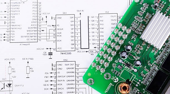
Understanding electrical schematics is essential for electronics professionals, as it connects design, testing, and production processes, facilitating effective PCB implementation.
2025/12/09
TQFP packages optimize PCB layout with space efficiency, RoHS compliance, and high reliability, addressing die shrinking and enhancing portability.
2025/02/17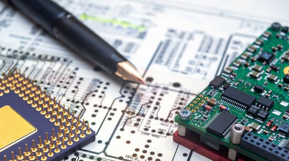
PCB schematics map circuit connections, while layouts focus on physical design for manufacturing. Both stages ensure optimal and reliable PCB design.
2025/02/11
The dielectric constant in PCBs affects signal speed, integrity, and impedance, crucial for optimizing high-frequency circuit performance.
2025/01/20
Nets in PCB design ensure logical connections from schematics to layout, enabling connectivity checks, design validation, and optimized manufacturing processes.
2024/12/05
PCBs are crucial in transforming energy grids into smart, efficient systems, optimizing renewable integration and energy management for a sustainable future.
2024/11/14
Select aluminum PCBs for excellent heat management or FR4 PCBs for cost-effective versatility in diverse electronic applications.
2024/11/12