
- Products & Capabilities

- About
- Resources
A Practical Guide to Quality Control and Testing in Bare PCB Production


Learn key quality control & testing workflows for bare PCB manufacturing. Understand AOI, flying probe, IPC standards to ensure circuit‑board reliability.
An unpopulated substrate equipped with copper traces, vias, pads and dielectric layers, also known as a printed circuit board (PCB), is the basic carrier used in almost all electronic equipment, ranging from consumer electronics to high performance aerospace systems, as well as medical instruments and industrial control devices. The bare board fabrication is a series of high precision procedures that involves lamination, drilling, plating, imaging, etching, solder mask coating and final surface finishing. Each manufacturing process presents a real danger of all sorts of defects, including: broken traces, hidden short circuits, uneven plating thickness and interlayer delamination. Unless defectives bare boards are carefully screened before assembly into components, they will cause signal disorder, unexpected hardware failures and possibly safety problems in end products. Thus, a full quality check and multiple testing is crucial in order to ensure the overall performance, yield rate, and long-term reliability of bare boards.
Full‑Process Quality Control Workflow
The quality management of bare boards is a closed loop system, which can be divided into raw material input, on‐site production monitoring and pre‐mass production verification.
Incoming material inspection is the first critical checkpoint. The raw materials for all copper-clad laminates, prepregs, solder mask ink and surface treatment chemicals must meet UL, RoHS and appropriate IPC requirements. Supplier certification documents are thoroughly checked, copper foil thickness uniformity is inspected and substrate flatness and surface condition are checked, and all materials that are not qualified or contaminated will be rejected, thus eliminating quality risks at the source.
Continuous in-process sampling is used to track critical production steps during the production process. Technicians manage drilling accuracy and burr size, monitor etching accuracy to prevent copper or short circuit residue, and ensure dust free workshop and stable temperature/humidity to prevent the surface of high-density fine-line multilayer boards from being polluted and pattern distortion. Formal mass production is always preceded by first article inspection (FAI). All first completed boards are completely dimensionally and electrically measured and all data are compared with original design drawings. Only after being corrected and parameters fully adjusted, and validated can batch production be allowed to commence.
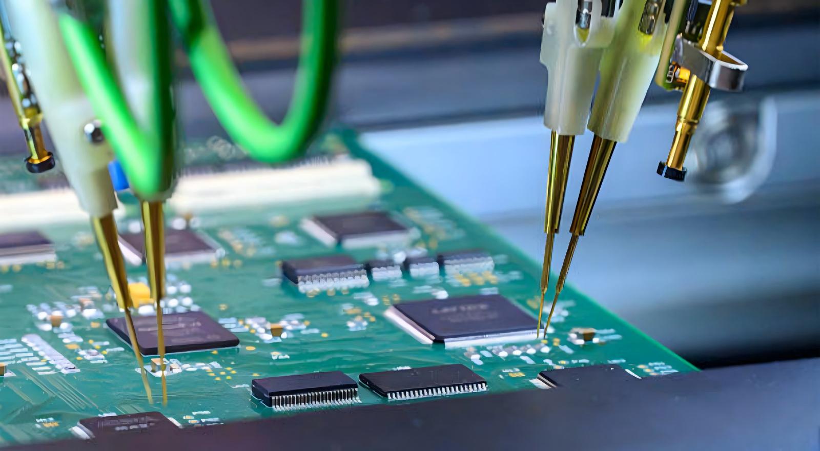
Core Testing Methods for Finished Bare Boards
Once all fabrication processes are finished, a series of complementary testing technologies are used to fully check the surface appearance, electrical functions and internal structural conditions.
After etching and solder mask processes, Automated Optical Inspection (AOI) is used extensively. Combined with cameras with high resolution and intelligent image comparison algorithms, AOI can automatically detect visible defects like trace breaks, solder mask misregistration, surface scratches, missing copper and residual copper shorts, etc., effectively overcoming the defect of being unable to conduct inspections for a long time due to visual fatigue.
The most important functional verification to check for open and short circuits is Electrical continuity and isolation testing. There are two mainstream testing modes: flying probe testing which is used when the prototype development or small batch orders, with frequent changes of circuit designs; Bed of Nails testing which is used when large volume mass production, with circuit designs being fixed.
When detection is not possible, all internal defects are analyzed by regularly taking microsections and performing cross‑section analysis in a destructive manner. Board samples are cut and polished and are examined under the microscopes to verify such major lurking issues that would cause the life span of high reliability bare board to shorten such as plating voids, inconsistent via copper thickness, interlayer delamination, and multilayer misalignment. In the meantime surface finish inspection is used to prevent possible solderability problems later in the assembly of components caused by contamination of the surface, typically of main stream finishes such as ENIG, HASL and OSP by oxidation. There will also be high-speed radio-frequency bare boards for added impedance testing to reduce signal attenuation and distortion during signal transmission.
Industry Standards and Future Development
All quality control and testing are performed in accordance with the common global IPC specifications, primarily IPC‑A‑600, visual acceptance standards, and IPC‑6012, rigid PCB performance requirements. Based on application use, bare boards are divided into three reliability classes: Class 1 for low demand consumer electronics; Class 2 for commercial and industrial equipment; and Class 3 for the high reliability levels of aerospace, medical and automotive safety hardware. All testing devices are calibrated regularly and complete sample test batch records are kept to achieve full quality traceability for customers' review and audit.
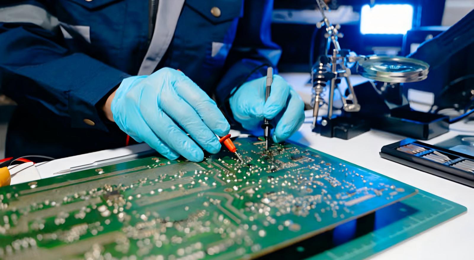
As electronics become smaller and smaller, and circuits more and more extremely fine, the traditional testing methods are increasingly challenged to detect the even smaller micro-defects. The whole industry is moving towards intelligent and digital quality inspection: AI algorithms enhance the AOI recognition accuracy and further reduce the false judgment rate; digital quality management platform analyses the real-time production data to predict the deviation of parameters, and changes the quality inspection from passive screening of defects to proactive prevention of risks. Integrated multi-functional testing machines are also more popular, which can be used for appearance, electrical and dimensional detection and improve the overall production efficiency of the factory.
Qualified bare board manufacturing is basic guaranteed by strict quality control and systematic test. All inspection links intercept possible defects, level out batch consistency and satisfy international reliability requirement from raw material testing to multiple dimensional finished board testing. Engineers and enterprises looking for standardized, high precision bare board with complete testing records, PCBX offers comprehensive testing solutions and quality control systems for the whole processes to ensure stable and durable performance for various kinds of electronic terminal products.
Hot Tags:

Contact us

If you can't find what you're looking for, please contact us.
Article
Prototype PCBs are essential for testing designs affordably and quickly, ensuring compatibility with modern tech. Effective documentation and design are crucial.
 2025/06/17
PCB reliability tests ensure performance under stress, reducing costs, enhancing product life, and meeting industry standards for quality and safety.
2024/12/17
Bare PCBs are unpopulated boards for component assembly. Zero PCBs, used for prototyping, allow custom designs. Both serve different roles in electronics.
2024/10/31