- Products & Capabilities

- About
- Resources
Copper Weight in Printed Circuit Boards (PCBs)


Copper weight determines PCB effectiveness in conductivity, thermal management, and mechanical strength, essential for high performance in various applications.
Printed Circuit Boards (PCBs) are the components of almost all electronic products, enabling complex circuitry to function with efficiency and reliability. Copper weight is a critical aspect of the design and performance of PCBs, an element which has an overarching influence on the board's electrical and thermal performance. The article presented here is a comprehensive discussion on copper weight in PCBs, its importance, and its implications for various electronic applications.
Copper Weight in PCBs
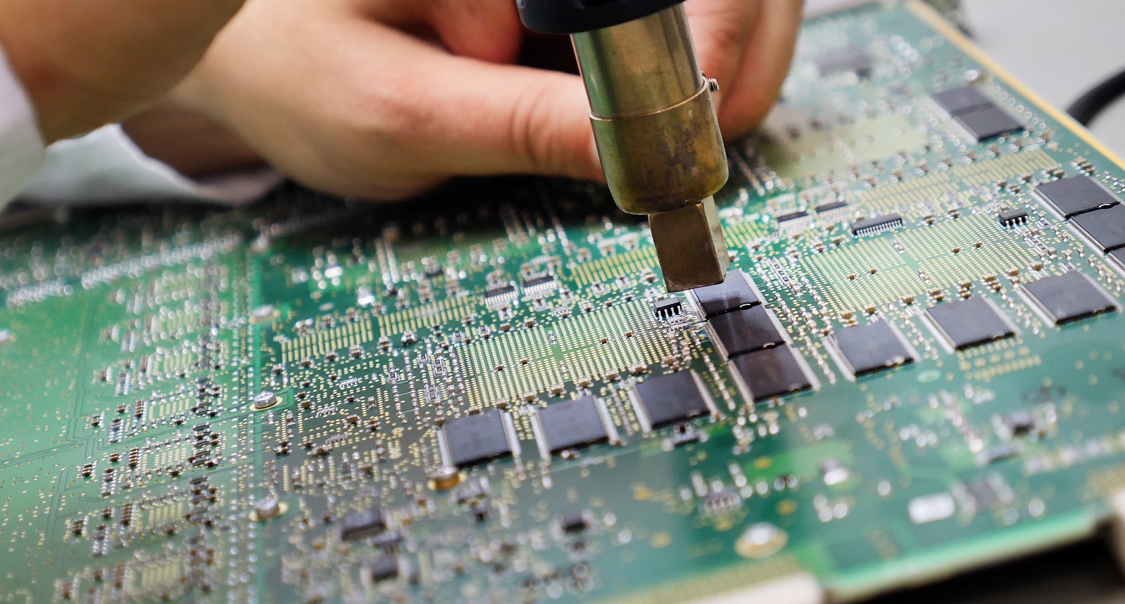
Copper weight in PCBs refers to the thickness of copper foil laminated on the substrate material. Usually measured in units of ounces per square foot (oz/ft²), copper weight can be converted into thickness, where 1 oz/ft² is approximately equal to 1.37 mils (thousandths of an inch) or 35 micrometers. It is a significant factor in how a PCB handles electrical currents, heat dissipation, and mechanical stability.
Copper Weight Importance
Electricity Conductivity: One of the key purposes of the copper trace on a PCB is to conduct electricity efficiently. The copper weight determines the cross-sectional thickness of the conducting traces, which decides the capacity of current that the board can efficiently carry. Higher copper weights support thicker conducting traces to carry higher amounts of current, required where high amounts of power are being transferred.
Thermal Management: Accurate thermal management is important in ensuring maximum performance and life of electronic devices. Increased copper weights ensure greater thermal dissipation, a vital property in PCBs used in high-power designs. Proper heat dissipation with heavier copper weights avoids overheating, protecting delicate electronic components from thermal stress and device reliability.
Mechanical Strength: Copper weight also contributes to the mechanical strength of the board. Thicker copper layers simply give more support, and the PCB is less susceptible to physical stress met during either the manufacturing process or end-use operation. This is particularly important in applications exposed to mechanical vibrations or thermal cycling, such as automotive or industrial environments.
Signal Integrity: Signal integrity is crucial in high-frequency applications. The copper weight of a PCB determines impedance and signal loss, or attenuation, along the conductive paths. Adequate thickness of copper ensures minimal signal loss, which is necessary for applications that require precise data transmission, such as RF circuits and high-speed digital circuits.
Common Copper Weights in PCB Design
PCBs can be made with varying copper weights depending on their application and performance requirements:
1 oz/ft²: This is the standard copper weight for the majority of consumer electronics and other products with modest power requirements. It offers a compromise between performance and cost, which is suitable for mass production where economic viability has to be ensured.
2 oz/ft²: Used in applications where higher current capacity and thermal management are required, such as power supply units and motor controllers. The additional cost in material is justified by improved reliability and performance, particularly thermal management.
Above 3 oz/ft²: Under conditions of excessive use, such as automotive, aerospace, and heavy industry usage, higher copper weights are appropriate. They call for high performance and endurance, and this is met by superior current carrying ability and heat transfer.
Design Parameters for Copper Weight
Copper weight designing is a balancing act based on numerous considerations:
Cost Management: Greater weights of copper, even though they bring performance benefits, add to the material and processing costs. Designers have to assess the cost-benefit ratio so that improved performance is worth the extra costs.
Space Constraints and Layout: The thickness of copper influences the overall layout of the PCB, specifically in products where the form factor is critical. It is important to properly design within space constraints so the device remains small and functional.
Challenges in Manufacturing: Larger copper layers create unique challenges in the manufacturing process of PCBs, such as the requirement of complex etching techniques and sustaining even adhesion between layers. These factors can complicate production and become costly.
Application-Specific Requirements: The selection of the copper weight should be related to the power, thermal, and performance requirements of the application. A thorough analysis of the operating environment and electrical parameters must be made to determine the optimal copper thickness.
Partnering with PCBX for Complex PCB Solutions
In advanced PCB manufacturing, it is important to know and utilize the correct copper weight to achieve optimal performance and reliability. PCBX excels in this regard, with unmatched knowledge and state-of-the-art technology, poised to cater to the diverse requirements of today's electronic designs. Whether your application demands regular or heavy copper weights, PCBX offers customized solutions meeting the best quality standards. Our focus on precision and innovation guarantees your electronic applications meet and surpass expectations in different industries. Opt for PCBX to benefit from our experience of converting your intricate needs into high-performance, efficient PCB solutions. With PCBX by your side, you not only enjoy the advantage of top-notch facilities and qualified technicians but also the assurance that you will be receiving PCBs professionally designed with copper weight and overall functionality in mind.
Hot Tags:

Contact us

If you can't find what you're looking for, please contact us.
Article
Heavy copper PCBs enhance current capacity and thermal performance, essential for high-power applications in military, automotive, and energy sectors, offering strength and heat dissipation.
 2024/10/21
PCB copper plating is key for creating conductive traces that drive electronic circuits, offering benefits like conductivity, anti-corrosion, and cost-effectiveness. Plating methods include electroless and electrolytic.
2024/09/25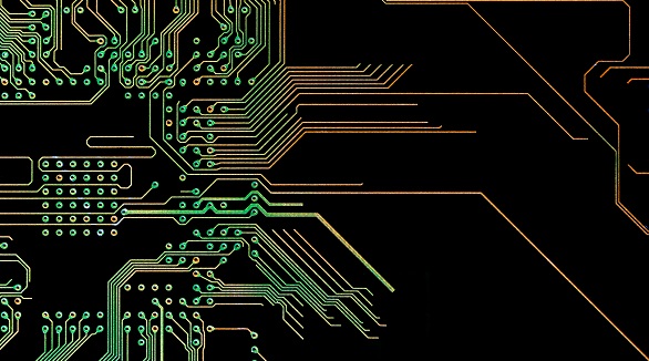
PCB trace technology is crucial for modern electronics, ensuring reliable and efficient signal transmission. Key elements include trace width, spacing, and material selection.
2024/09/25