- Products & Capabilities

- About
- Resources
Trace-to-Pad Clearance in PCB Design


Proper trace-to-pad clearance in PCB design ensures safety, signal integrity, manufacturability, and longevity, following standards like IPC 2221 for optimal performance.
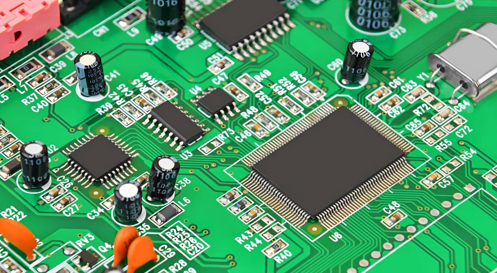
PCB design is a very important procedure in the development of electronic equipment, as it determines the performance and reliability of the electronic device. Trace-to-pad clearance is among the most important things to consider when designing PCBs. This is a factor that is usually ignored and may greatly affect the integrity and efficiency of a PCB.
Understanding Trace-to-Pad Clearance
Trace-to-pad clearance is the minimum distance separating a PCB conductive trace and a pad. Evidence Pads are metal spots used to attach components Traces are routes of electric signals. It is important to make sure that there is proper distance between all these components to avoid any electrical short-circuing, signal distortion or even possible arc in high voltage applications.
Significance of Trace-to-Pad Clearance
Safety and Reliability: One of the major causes of maintaining good trace-to-pad clearance is to provide safety, especially in high-voltage designs. Inappropriate clearance may cause arcing that may result in short circuit, fires or component damage. On following the correct spacing, you are enhancing safety as well as reliability of the PCB in the long run.
Signal Integrity: In fast digital circuits, the distance between the traces and pads is too low, resulting in crosstalk, in which signals interfere with each other, causing poor performance. Proper clearance also reduces such risks and maintains the signal integrity and the accuracy of data.
Manufacturability: These are the tolerances in spacing, which are determined by the capabilities of the equipment used by PCB manufacturers. Designs falling short of these tolerances may cause delays in production, cost increases or even fabrication flaws. Proper clearance means that the design matches the manufacturing capabilities which make the production easier.
Long-Term Performance: The moisture, dust, and thermal variations are some of the environmental factors that can affect the lifespan of a PCB. Trace-to-pad clearance Adequate trace-to-pad clearance helps to minimize the chances of environmental effects that can cause deterioration or failure, and make the circuit board have a useful lifespan.
Industry Standards: IPC 2221
The IPC 2221 standard is a full guideline on trace spacing so that guide designers on the right clearances. It takes into account the level of voltage and environmental conditions and makes sure that the designs are safe and reliable.
Voltage Levels: The standard provides certain recommendations depending on the voltage levels whereby, low voltage has the lowest clearance and the higher the voltage the higher the clearance to ensure prevention of dielectric breakdown.
Environmental Factors: Another environmental factor that IPC 2221 recommends is alteration due to other conditions like altitude and humidity which can impact the dielectric strength of a board and may require higher clearances.
Identifying Appropriate Clearance
Voltage Requirements: Determine the highest voltages differentials in your design. This assists in setting a standard against which the required clearance should be made with references to IPC 2221 or any other standard.
Environmental Conditions: Assess the working conditions of the PCB, including such aspects as humidity and altitude. Modify the clearances to fit the conditions that might otherwise lower the dielectric strength of the board.
Meet Manufacturers: It is important to work with PCB manufacturers at an early stage. Their capability and limitations in production make you know that your design is possible and that it will be practical to be fabricated.
Signal Speed: When using high frequencies, clearance sizes can be greater to avoid crosstalk and signal distortion. Simulate design software to forecast and avoid possible interference.
Material and Coatings: The material and coating (e.g. solder masks) may influence the necessary clearance. Sometimes coated boards are used with a lower spacing, as more insulation is provided.
Optimizing Your Design
Use Design Rule Checks (DRC): Use advanced PCB design software to develop and enforce clearance rules. This aspect can automatically identify and mark violations and can respond to possible problems at the initial stages of design.
Prototype and Validate: Prototyping is necessary before proceeding to mass production. The step presents an opportunity to check your design assumptions and ensure that the spacing is satisfactory in real life scenarios.
Implement Best Practices: Use uniform spacing in the design and keep similar net classes together, as well as isolate high-voltage sections and maintain a sufficient distance between them and inaccessible to low-voltage sections.
Plan for Multi-layer Designs: With a space limitation, multi-layer boards should be considered to isolate high voltage or high-speed traces to reduce clearance considerations.
Avoiding Common Mistakes
These are the pitfalls to avoid to come up with a strong design:
Failure to follow Voltage Consideration: The failure to take into account voltage level factors can lead to insufficient clearance and higher levels of arcing.
Ignoring Environmental Impact: Insufficient estimation of conditions (such as humidity or the altitude) could be the cause of an insufficient distance and possible reliability problems.
Ignoring High-Speed Effects: In high-frequency designs, an unaccounted signal integrity can harm the performance by creating unwanted interference.
Neglect of Creepage: In addition to having proper clearance (air gap), creepage (surface distance) is also important in eliminating shorts caused by surface contaminants.
Clearance of traces to pads is an element of mastering effective, safe and dependable PCB designs. Learning its significance, following the industry standards such as IPC 2221, and taking into account the effects of environmental and manufacturing conditions allows the designers to develop the PCBs that will comply with the utmost quality criteria. By using the information and tips presented in this guide you will be able to get through the mazes of PCB design, having strong layouts which may endure the requirements of current electronic applications.
Hot Tags:

Contact us

If you can't find what you're looking for, please contact us.
Article
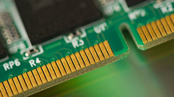
Edge connector bevelling enhances PCB durability and reliable connections, vital for frequent usage and secure engagements, with limitations primarily in plating.
 2024/12/25
Power and ground planes in PCBs ensure signal integrity, manage heat, and minimize EMI, crucial for efficient, high-performance electronic devices.
2024/11/11
DFM ensures cost-effective PCB design by optimizing size, layers, materials, and components, focusing on manufacturability, reliability, and process efficiency.
2024/10/30