- Products & Capabilities

- About
- Resources
Copper Balance in PCB Fabrication


Copper balance is key in PCB fabrication, ensuring signal integrity, thermal management, and reliability by managing copper distribution for efficiency.
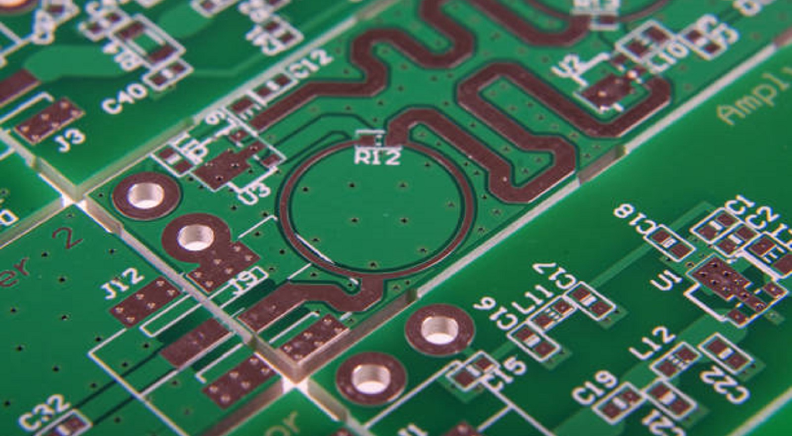
In today's quick electronic world, PCB manufacturing is a critical process that needs to be highly accurate. Everything depends on achieving the best copper balance—a critical factor whose direct influence is on the final product's quality, functionality, and reliability. Copper balance incorporates precise control and management of copper distribution within PCB layers so as to achieve the required copper thickness and patterns in the manufacturing process.
Comprehending Copper Balance
Copper balance is essential in PCB production for many reasons:
Signal Integrity: Consistent copper thickness and balanced distribution are necessary for maintaining signal integrity, preventing signals from being distorted, crosstalk, and electromagnetic interference (EMI). Copper balance ensures that the electrical path behaves as intended, with data integrity and device performance.
Thermal Management: Adequate balance of copper facilitates effective heat dissipation and prevents hot spots that may cause component failure or damage. Reduction of thermal stress extends the life and reliability of the PCB.
Reliability: Uneven copper distribution may result in local stress concentration, which increases the likelihood of defects such as delamination and cracks. Such defects make the board unreliable and less robust, and it can suffer operational failure.
Manufacturing Yield: A perfect copper distribution reduces occurrences of defects and hence provides improved manufacturing yield and reduced wastage. This not only enhances production efficiency but also gives assurance for less rework cost and material wastage.
Factors Influencing Copper Balance
Copper Plating Process
The process of copper plating has the greatest controlling influence on copper distribution on the PCB. The critical parameters are:
Composition of Plating Bath: The composition of the bath, i.e., copper ion concentrations, additives, and other chemicals, controls the effectiveness of the rate of plating along with uniformity. Unequal composition of the bath can lead to uneven deposition or defective plating.
Current Density: Current density at the plating time determines the copper deposition rate. It is absolutely necessary to have constant current density across the whole PCB surface to achieve uniform copper thickness.
Plating Time: Plating time regulates overall copper thickness. Effective control on plating time is very important in order to achieve desired copper thickness with minimum risk of over-plating and under-plating.
Panel Design and Layout
The PCB design and layout play an important role in copper balance.
Trace Patterns: Complex trace patterns or high-density interconnects could lead to local areas of increased or decreased copper concentration, causing imbalances in copper distribution.
Copper Area Distribution: Copper area placement, planes, pads, and traces impact current density and plating rates, and variations in copper thickness are likely to occur due to the above reasons.
Panel Panelization: Subdivision and subdivision of PCB panels have the potential to influence current distribution and plating uniformity, especially on the edges and corners of the panel.
Plating Equipment and Setup
Equipment setup of plating, fluid flow, and distribution of electrical fields are major factors to maintain copper balance.
Anode Configuration: Anode position, shape, and quantity in the plating tank control the current distribution and plating uniformity across the PCB panel.
Fluid Dynamics: Turbulence and flow patterns within the plating solution control copper ion and additives mass transfer, leading to variations in copper thickness and plating rates.
Electrical Field Distribution: Electrical field distribution within the plating tank is critically important in creating current density and plating uniformity on the PCB panel.
Methods of Copper Balance Maintenance
Optimization of the Plating Process
Plating Bath Monitoring and Adjustment: Ongoing monitoring and adjustment of the composition of the bath is essential to ensure uniformity and steady plating rates.
Current Density Control: Employ advanced current control systems to maintain uniform current density on the whole PCB panel surface, considering trace pattern variations and copper area distribution.
Plating Time Monitoring: Proper monitoring and control of plating time guarantee achievement of the required copper thickness with minimum over-plating or under-plating.
Panel Design Optimization
Copper Area Balancing: Positioning of copper areas on the PCB panel in a manner that keeps current density variations to the minimum and plating rates uniform.
Panelization Optimization: Proper consideration of the panel panelization method ensures minimum edge effect influence and even current distribution across the entire panel.
Plating Equipment Enhancements
Anode Configuration Optimization: Employ innovative anode configurations, such as auxiliary anodes or shielding, to encourage more uniform current distribution and plating rates across the PCB panel.
Fluid Dynamics Optimization: Employ high-end agitation systems or flow-controlled plating cells to achieve the highest possible mass transfer of copper ions and additives, with uniform plating rates across the panel.
Electrical Field Shaping: Apply electrical field shaping techniques, including the use of thiefing shields or auxiliary electrodes, to mold the electrical field distribution and promote uniform current density across the PCB panel.
In-Line Monitoring and Feedback Control
Employing advanced in-line monitoring and feedback control systems will significantly enhance copper balance by allowing for real-time adjustments and corrections during ongoing plating:
Thickness Monitoring: Thickness monitoring in-line can be achieved by eddy current and optical sensors. These monitors constantly assess copper thickness on the PCB panel.
Feedback Control Systems: Incorporate feedback control systems that would render plating parameters automatically adjustable, for example, by varying the current density and plating time or bath composition, based on real-time thickness measurement to ensure copper is evenly distributed throughout the entire plating operation.
These practices allow PCB manufacturers to balance copper, achieving maximum performance and reliability at reduced waste and cost. PCBX specializes in such techniques, providing high-quality PCBs to meet stringent industry demands.
Hot Tags:

Contact us

If you can't find what you're looking for, please contact us.
Article

Populated circuit boards integrate electronic components for efficiency and reliability, utilizing SMT and THT for diverse applications across industries.
 2024/12/17
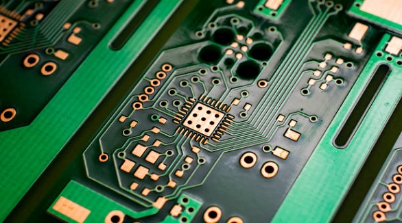
3 oz copper PCBs are rising in popularity due to enhanced conductivity, thermal management, and durability for high-power applications, despite added costs.
2024/11/18
PCB copper plating is key for creating conductive traces that drive electronic circuits, offering benefits like conductivity, anti-corrosion, and cost-effectiveness. Plating methods include electroless and electrolytic.
2024/09/25