- Products & Capabilities

- About
- Resources
What is SMT Footprint?


SMT footprints are critical PCB designs for mounting components directly, ensuring electrical connections and standardization, aiding efficient manufacturing.
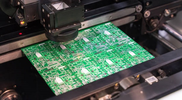
In today's ever-evolving world of electronics design, Surface Mount Technology (SMT) is a groundbreaking method in printed circuit board assembly that has replaced the traditional through-hole procedures. The method allows components to be mounted on the surface of printed circuit boards (PCBs) directly, and the concept of SMT footprint becomes the focal point. This article aims to explore SMT footprints in detail, its significance, design, and structure, and the design practices that must be followed by electronics engineers and PCB designers.
What is an SMT Footprint?
An SMT footprint is essentially the PCB design that defines how each component is physically mounted and electrically connected. Composed of an array of different elements, the footprint is critical for assembly and function. The main items are:
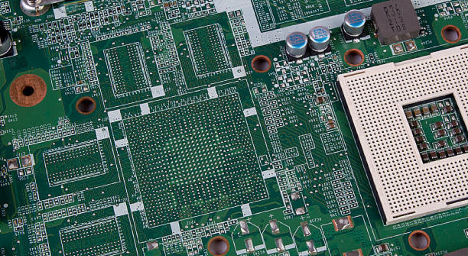
Pads
These copper areas form the principal contact points for electric signals, bonding a component's terminals to the conductive traces on the PCB.
Solder Mask Openings
These are openings above pads that expose them to solder and offer insulation for the remainder of the board, ultimately controlling solder application.
Silkscreen Outlines and Text
Visual pointers such as silkscreen prints and text help in correct positioning and orientation of components, with identification marks on them at assembly.
Fiducials
Fiducials are employed as optical alignment references for automated assembly machines, e.g., pick-and-place machines, that are common in mass production equipment.
The SMT Footprint Architecture
SMT footprint architecture must be precise in order to ensure maximum mounting of parts, including several important aspects:
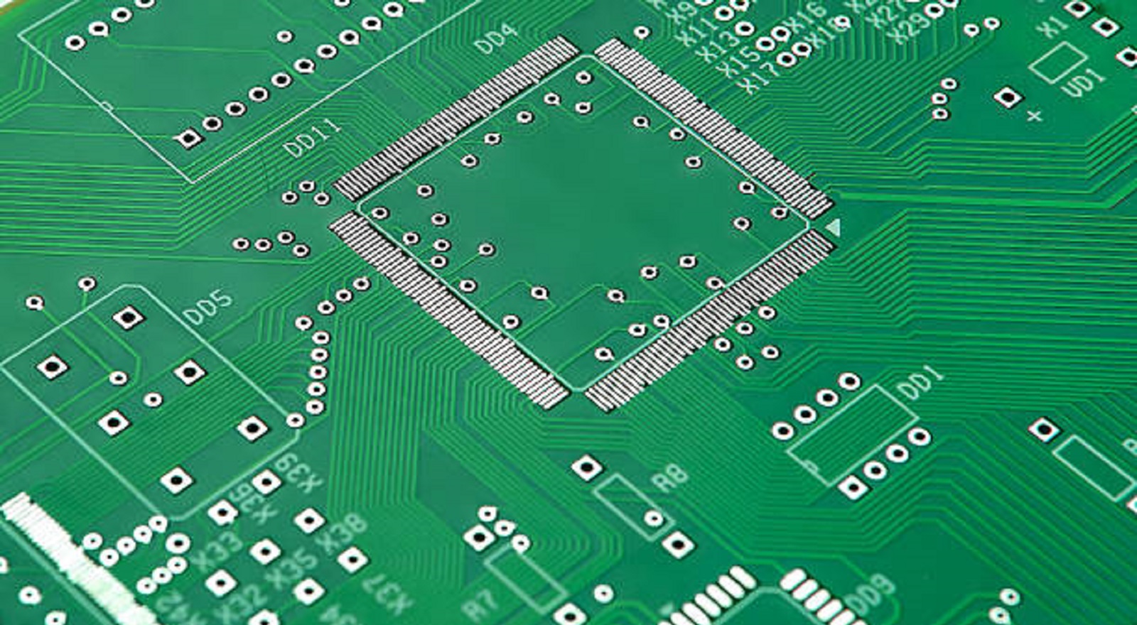
Pad Geometries and Sizes
Pads come in various shapes of geometry that are intended to accommodate a number of components and uses:
Rectangular: Most common, for perimeter leads on components.
Rounded Rectangular: Rounded corners to reduce stress concentration.
Oval: For high pitches down to 0201 sizes, with sufficient solder volume.
Square: For area-array components like BGAs (Ball Grid Arrays).
Donut: Ring-pads for visual solder inspection uses.
Pad size dimensions are length, width, corner radii, and thickness of finished copper. For instance, standards such as IPC-7351 provide dimensional guidelines to match pad size with component leads to ensure stable solder joints.
Solder Mask Openings
Critical to the accurate application of solder and minimizing bridging, solder mask openings are typically 25-100 μm larger than pads. This allows for alignment tolerance without raising the chance of solder bridging.
Orientation and Specialty Pads
Orientation guides, such as polarity markers and fiducials, are critical to inserting the component correctly. Specialty pads address special package needs:
Thermal Pads: Efficient at carrying heat away from the component
Castellated Pads: For MEMS and LED packages with edge extension of pads
Compliant Interface Pads: Provide stress relief for components mounted to a rigid PCB.
The Importance of Standardization
Standardized footprints from large libraries of PCB software deliver several benefits:
Reliability and Consistency: Ensures all dimensions adhere to component specifications, leading to consistent assembly.
Interchangeability: Allows for substitution of similar components from different manufacturers.
Reuse of Design: Enables reuse of tested footprints in multiple designs, saving time and resources.
Manufacturability: Ensures conformance to defined fabrication processes.
Non-standard custom footprints are sometimes unavoidable to accommodate innovative or proprietary package designs, however.
Design Guidelines for Optimizing SMT Footprints
Creating good SMT footprints involves best practices for creating strong, manufacturable designs:
Pad Sizing Accuracy: Size pads to be equal to component leads with adequate manufacturing tolerances. Avoid oversized pads that can lead to solder bridging.
Rounded Corners: Incorporate rounded pad corners to minimize solder voiding.
Good Orientation Markers: Incorporate silkscreen outlines, text, and fiducials for component alignment.
Solder Mask Expansion: Open slightly larger areas than pad size for easier soldering without the risk of solder bridging.
Thermal Management: Connect large pads to inner layers to assist in heat dissipation, which is crucial for high-power components.
Consider Rework/Repair: Design for ease of access to make any rework or repair simpler.
Validation: Always verify designs with manufacturer specifications and adhere to industry standards.
SMT footprint design is still an important part of the PCB layout and manufacturing operations. By gaining the subtlety of footprint design, engineers would be able to gain reliability, efficiency, and manufacturability, all very much for creating electronic devices that are satisfying the needs of the times. As components get smaller and electronic systems more and more complex, the understanding and utilization of efficient SMT footprint design principles would be at the uppermost level of importance in fostering innovation and success of electronic product development.
At PCBX, we strive to provide engineers with the information and tools necessary to increase their understanding of cutting-edge PCB design practices. As SMT becomes the wave of the future in electronics manufacturing, the role that well-designed footprints will play will become more valuable, paving the way for innovation and breakthroughs in products within the arena of electronics. By keeping pace with evolving design techniques, manufacturers can ensure their products stay at the leading edge of technology, offering greater performance and dependability in increasingly smaller devices.
Hot Tags:

Contact us

If you can't find what you're looking for, please contact us.
Article
FAI in SMT ensures product quality by detecting defects early, using methods like AOI and X-ray, ultimately enhancing efficiency and customer trust.
 2025/06/26
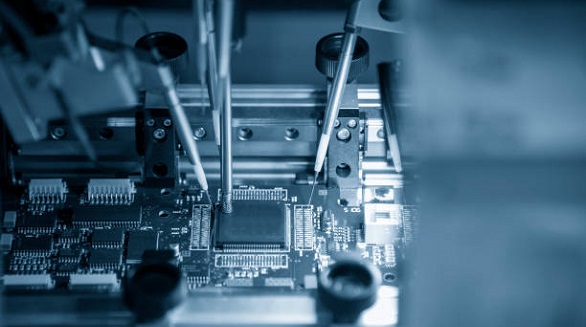
SMT enables miniaturization in electronics manufacturing but presents defects that need identification and resolution to ensure product quality and efficiency.
2025/06/19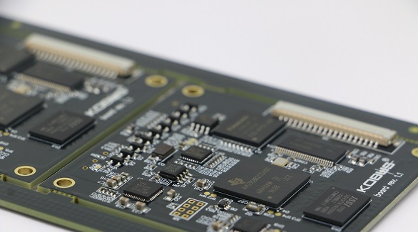
SMT assembly places components directly on PCBs, enhancing miniaturization, performance, and efficiency. Key steps: solder paste printing, chip mounting, reflow soldering, and inspection.
2024/08/05