- Products & Capabilities

- About
- Resources
What is BGA Chip?


BGA chips offer compact, high-performance mounting for PCBs, essential in modern electronics, but require precise handling and advanced inspection methods.
In today's high-speed electronic world, the Ball Grid Array (BGA) chip is an essential technology employed for mounting integrated circuits on printed circuit boards (PCBs). At PCBX, we realize the critical role that BGA technology plays towards enhancing device reliability and functionality. This article discusses the components of BGA chips, such as their structure, advantages, applications, and some of the issues that they present, giving reasons why they are widely favored in the electronics industry.
Definition and Structure
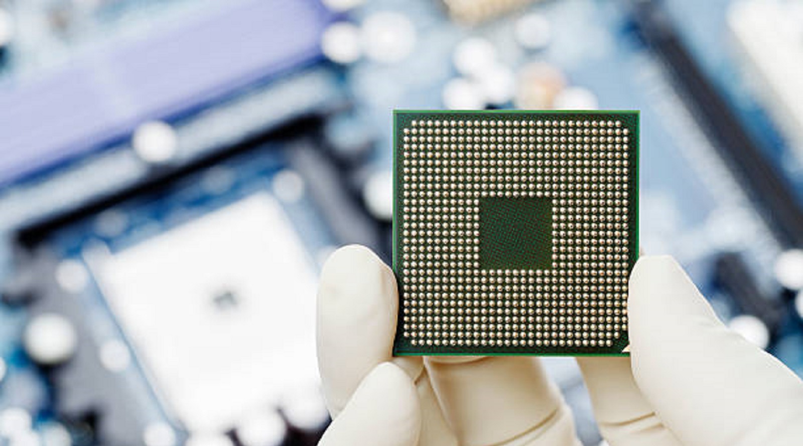
A Ball Grid Array (BGA) is a surface-mount technology that uses an array of solder balls instead of pins to form electrical connections. This configuration optimizes space and improves electrical performance with the concentration of all the contacts at the bottom side of the chip. BGA is also referred to as a Chip Size Package (CSP) due to its small size and efficient design despite the fact that BGAs can be applied to more complex configurations, including multi-chip and flip-chip configurations.
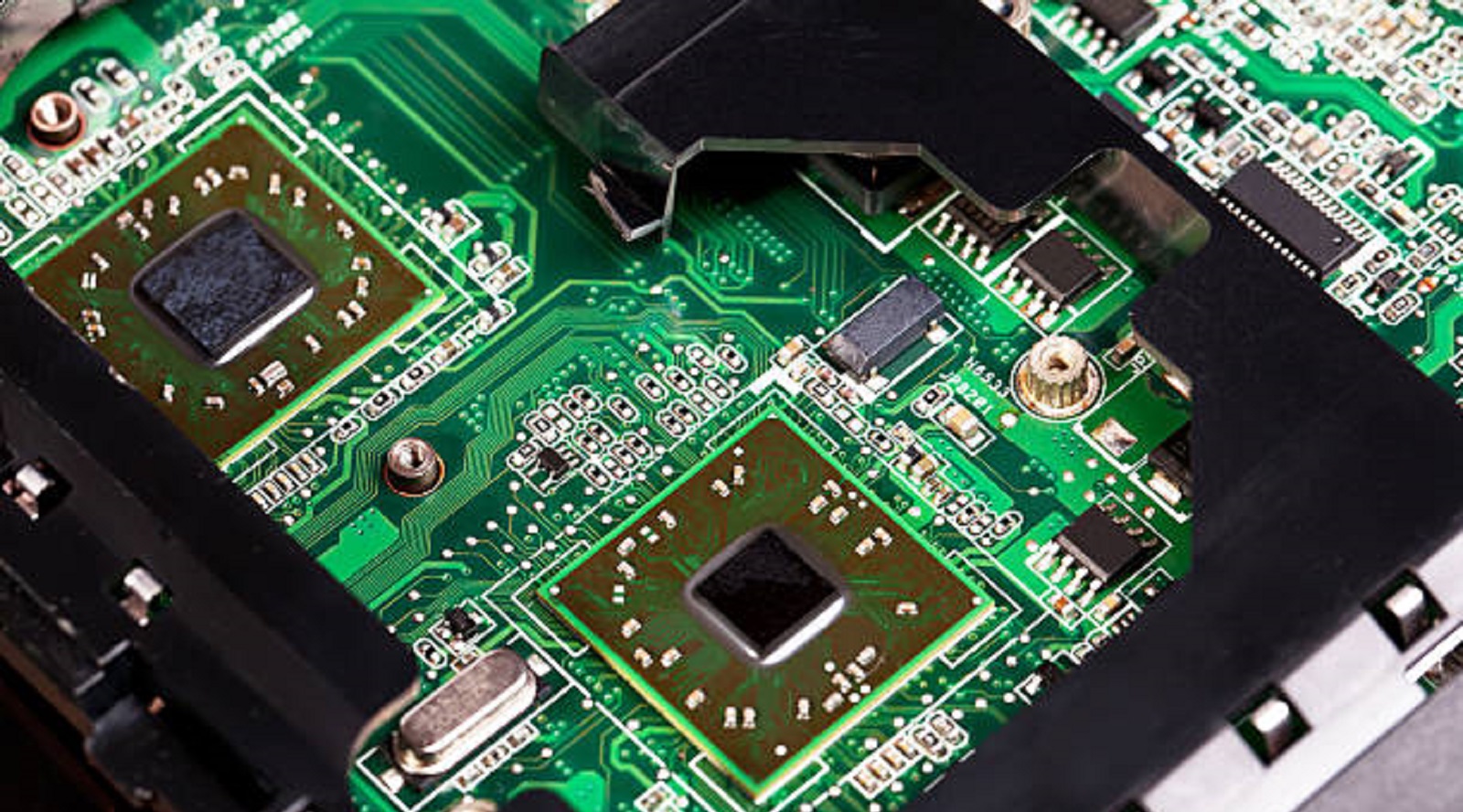
The unique BGA form consists of solder balls packaged into a grid array fashion on the backside of the chip. The balls are processed under reflow, whereby the balls are heated to extremely high temperatures above 400°C (750°F) to form robust joints with the PCB. Reflow reinforces mechanical and electrical reliability of the joints, which is important for ensuring the functionality of high-performance electronic devices.
Distinguishing Features
BGAs have the following characteristic features:
Miniature Package: BGAs occupy only approximately 1/20th the size of similar pin-based packages, equating to enormous space savings. Small size provides more design freedom and accommodation of more functionality in smaller space.
Single-Surface Connects: All electrical connects are on the bottom surface of the chip, with a smaller PCB footprint and allowing more circuitry to be packed in.
Ball-Based Interfaces: Interfaces are created using solder balls instead of wires, which provides higher mechanical strength. The balls are accommodated within small misalignments, so mechanical damage is less probable during the assembly process.
Advantages of BGA Chips
The design and structure of BGAs impart various advantages over other packaging technologies:
Improved Electrical Performance:
The compact electric paths in BGAs reduce inductance, enhancing signal speed and dependability, essential in high-frequency applications.
Better Thermal Management:
The design offers better heat dissipation, which is essential for devices operating at high temperatures or power levels. This thermal efficiency contributes to the longevity and reliability of electronic components.
Optimum Space Utilization:
High density of connection allows BGAs to support dense designs, ideal for space-constrained devices such as smartphones, tablets, and wearable tech.
Mechanical Robustness:
The robust mechanical coupling provided by the solder balls helps the connection to be more robust and less susceptible to mechanical stress failure.
Applications of BGA Chips
With their extensive benefits, BGA chips have numerous applications in various industries:
Consumer Electronics: BGAs play an integral part in devices such as mobile phones, laptops, and tablets, providing the processing power and functionality required without compromising on space.
Automotive Systems: In premium car electronics, BGAs are vital for high-speed, efficient data processing to support features such as infotainment systems, security features, and autonomous driving capabilities.
Medical Devices: Medical devices requiring precision, reliability, and high-performing robustness are greatly advantaged by the increased capability of BGAs.
Telecommunications and Networking: Network devices such as routers and switches employ BGAs because of their ability to carry high-speed data well.
Challenges and Considerations
Despite having a lot of benefits, BGA has some issues:
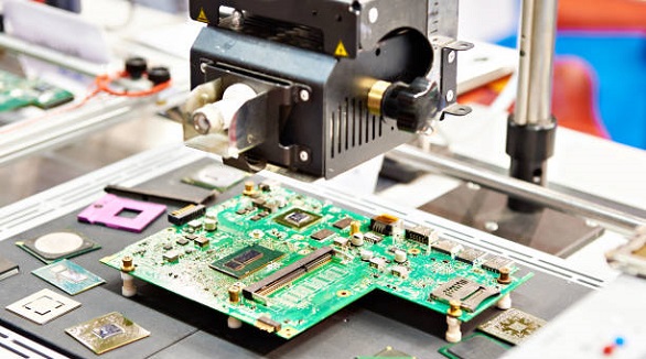
Inspection Challenges: The connections are below the chip, and ordinary visual inspection is inadequate. Special techniques such as X-ray inspection must be employed to confirm connection integrity.
Repair Difficulty: The complexity and size of BGAs make rework or repair more difficult. Specialized equipment and expertise are required for rework or replacement.
Cost Implications: The precision and technology required in BGA assembly can be prohibitively expensive. These costs tend to be recovered by the enhanced performance and dependability of the chip, however.
Heat Management: The significant heat involved with reflow soldering actually poses a risk to the substrate material at times. Proper heat dissipation and utilizing materials that can endure high temperatures are critical.
Solutions and Considerations
These issues can be addressed by manufacturers through some strategic changes. Soldering across the entire PCB and then reworking it through solder baths or hot air can improve feasibility, especially in high-volume or reliability use. It facilitates that skilled personnel work on surface-mount technology and can visually inspect following assembly. In high-reliability applications, using BGA sockets can make mounting and replacement processes easier.
Benefits of CSP Packages
BGAs are preferred to CSPs by manufacturers for a variety of reasons:
Smaller Package Size: BGAs generally consist of a smaller package size compared to their CSP counterparts.
Higher Packing Density: BGAs have higher packing density, which keeps the PCB shorter in height and utilizes space optimally.
Cost-Effectiveness: The smaller size and fewer components result in BGAs being economical to produce. In addition, robotic equipment can deposit the solder balls quickly and efficiently, improving manufacturing efficiency.
Shape Range: BGAs possess a wider range of shapes compared to CSPs, with design versatility and the option to utilize in devices.
BGA technology represents a huge advancement for the electronics industry, with a clear combination of performance, reliability, and miniaturization. As an option for companies looking for PCB alternatives, BGA chips are a compelling argument for use in today's device design and manufacturing. Through enabling smaller device footprints while supporting complex functionalities, BGAs play a key role in pushing the boundaries of what is possible in electronics. We at PCBX encourage careful consideration of BGAs in design specifications, appreciating their potential to define electronic development for the future. Get in touch with PCBX for customized manufacturing and assembly services that utilize the potential of BGA technology for your future projects.
Hot Tags:

Contact us

If you can't find what you're looking for, please contact us.
Article
BGA reballing restores functionality to failed solder joints using precise tools and methods, crucial for compact devices facing thermal, physical, or environmental stress.
 2025/04/29
The article compares Ball Grid Array (BGA) and Land Grid Array (LGA) packaging technologies for mounting microprocessors on PCBs. It details their pros and cons, applications, and factors to consider for optimal design choices.
2024/09/23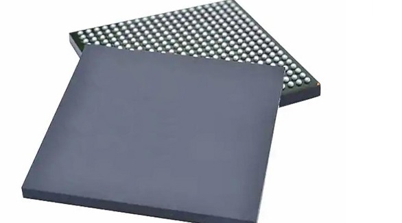
Compared to THT, SMT offers better miniaturization and weight reduction in any electronic application. With the use of BGA packages, high-assembly density, reliability, and improved performance are achieved; on the other hand, this requires a rework and inspection that is not really common. PCBX specializes in the area of advanced SMT and BGA assembly to help drive modern requirements of compact electronic devices.
2024/07/26