- Products & Capabilities

- About
- Resources
Designing a Motherboard PCB


Motherboard PCBs connect key components, like CPUs and memory, in electronic devices. They require precise engineering and testing for optimal performance across consumer and industrial applications.
The motherboard is that integral part of an electronic system-a computer, an electric device-that forms the connecting link for all parts that will function as units thereof. In this article, considerations are made, in great detail, regarding what a motherboard PCB entails concerning its elements and best practices to realize optimal performance.
Introduction to Motherboard PCB Design
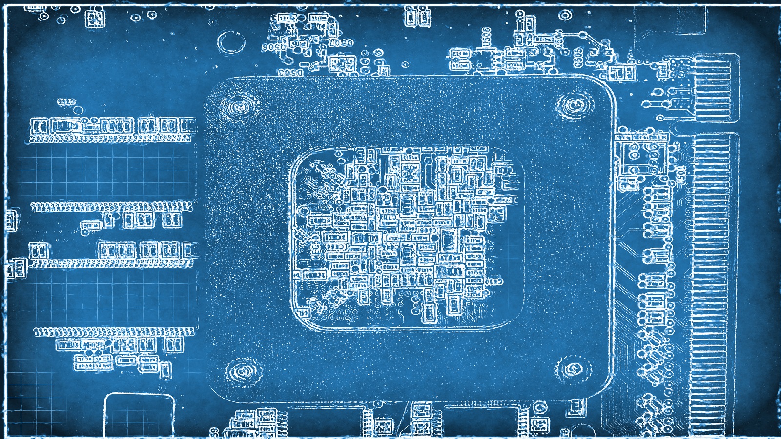
The motherboard PCB, also known as a logic board, system board, or mainboard, is a primary circuit board in computers and other expandable systems. It consists of many layers, often no less than four, with complex electrical connections using integrated circuits, passive elements, and connectors. These boards allow the communication of key components, such as CPU and memory, with other peripherals like storage devices and graphics cards.
Unlike a backplane, which is essentially a hub of connectors, the motherboard integrates these with core processing units and subsystems to form a basic platform of communication and synchronization for internal components of a device.
Key Components of a Motherboard PCB
Designing a motherboard involves understanding and positioning a number of components essential to system performance:
CPU Socket: It houses the CPU, which is considered the brain of the whole system. Proper placement and cooling of the CPU socket are needed for high and efficient processing.
DIMM (Memory Slots): These are the sockets for RAM, which provide fast, short-term data storage; hence, directly influencing the system speed and efficiency.
Chipset: Comprising Northbridge and Southbridge, the chipset is designed for managing communication between the processor, memory, and peripherals. Northbridge controls the high-speed channels, while the low-speed peripherals are controlled by Southbridge.
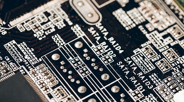
Expansion Slots: Similar to PCIe slots, these are for accommodating additional capabilities such as a graphics card, audio card, and NICs.
Power Connectors: These will connect the motherboard to the power supply of the computer.
Thermal Management Systems: These include heat sinks and fan mounts that help dissipate heat from high-energy components and preserve reliability and performance.
Input/Output Ports: Including but not limited to USB and audio jacks, these are used to connect other devices to the motherboard.
Motherboard PCB Design Steps
The designing of a motherboard PCB is a complex process that includes keen attention to detail both in planning and execution and is an amalgamation of engineering expertise with innovative solutions in design. The step-by-step processes will involve:
Initial Planning and Requirements Definition
Define the electrical, mechanical, and functional requirements; include component specifications and overall layout considerations.
Schematic Design
Develop a detailed schematic of what each connection is for and why. Use any software tools to create a virtual version of how components will interact with one another.
Component Placement
Place the components to reduce trace lengths and enhance wiring efficiency. Place high-power components such as the CPU close to power supplies to reduce voltage drops.
Signal Routing
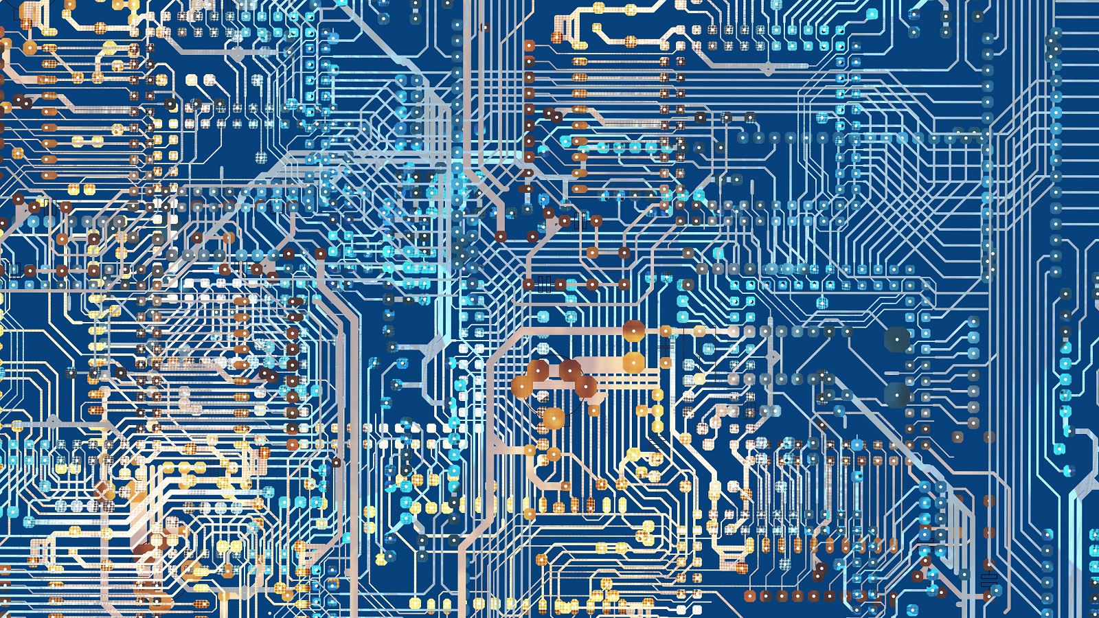
Differential pair routing for high-speed data paths, such as PCIe and memory interfaces, reduces interference.
Use micro-via technology to interconnect different PCB layers to reduce electromagnetic interference along with signal degradation.
Power Distribution Strategy
Utilize multiple power layers to evenly distribute power for minimum electrical noise and maximum efficiency.
Impose robust voltage regulation near high-power components to assure stable power delivery.
Thermal Management
Design for good cooling, considering airflow and including heat sinks and fan mounts as necessary to help dissipate heat generated by high-powered components.
Prototype Testing
Provide a prototype to validate functionality by series of stringent tests required to find and fix the design bugs before volume productions.
Automated testing with emulation to validate component functionality under a range of conditions.
Iterative Refinement
Improve the design through testing of prototypes to ensure the final product meets performance and regulatory standards.
How Motherboard PCBs Differ from Other Circuit Boards
While all motherboards are PCBs, not every PCB functions as a motherboard. Motherboard PCBs can easily be identified by their complex nature and capability to perform multiple functions. They consist of various copper layers separated by insulation that carries a great deal of components performing integrated functions of the system. Less complicated PCBs handle only a part of the workload of the device and may contain fewer layers.
Applications and Advantages
Motherboard PCBs are very important in many fields, starting from consumer electronics to industrial use:
Consumer Electronics: They organize the interaction of complex processes and functions within personal computers, smartphones, and smart TVs.
Industrial Applications: It forms a stern base in manufacturing machines or automation tools that make their work feasible in tough environments.
The biggest advantage of a well-designed motherboard PCB is the seamless, efficient operation it allows for complex systems, supporting multi-functionality while maintaining high performance.
Conclusion
A motherboard PCB involves precision engineering, an understanding of a wide number of components, and much testing to ensure that reliability and performance are met. Such a design ensures motherboards meet and advance technological expectations concerning reliability and efficiency through a wide array of applications. The motherboard PCBs will serve as the core foundation on which novel solutions can rest in various electronic applications-be it consumer electronics, industrial applications, or otherwise-if the principles of design and standards of the industry in general are adhered to.
Hot Tags:

Contact us

If you can't find what you're looking for, please contact us.
Article
Designing a PCB involves ten detailed steps: schematic capture, creating a blank PCB layout, syncing designs, defining stackup, setting design rules, placing components, adding drill holes, routing traces, labeling, and generating output files. These steps ensure an organized, error-free process from concept to manufacturing.
 2024/08/29
PCB prototyping is vital for testing and refining electronic circuits before mass production, ensuring performance and feasibility using methods like etching, milling, and 3D printing.
2024/08/13
The article is developed concerning the breakthrough of integrated circuits and the need for custom PCBs in some electronic products. It enumerates ten golden rules in conducting PCB layout design and manufacturing: grid selection, routing, power layers, component placement, panel duplication, component value combination, frequent DRC, flexible silkscreen use, decoupling capacitors, and pre-production parameter checks. These rules provide for the optimum design and manufacturing of a PCB.
2024/07/25