- Products & Capabilities

- About
- Resources
How to Design a Printed Circuit Board


Designing a PCB involves ten detailed steps: schematic capture, creating a blank PCB layout, syncing designs, defining stackup, setting design rules, placing components, adding drill holes, routing traces, labeling, and generating output files. These steps ensure an organized, error-free process from concept to manufacturing.
Designing a printed circuit board is an intensive, step-by-step process that requires a lot of thought, detail, and the right pack of tools. Here's the complete guide on how to take your ideas from concept to finished product with the help of the following ten important steps.
Step 1: Schematic Capture
This phase of schematic capture, you will begin to develop the blueprint stage, either starting with a template or creating a design from scratch:
Component selection: Select components according to the requirement of the circuit.
Symbols and Footprints: Either design or import, if necessary, schematic symbols and footprints.
Schematic Drawing: Place CAD tools drawing on the schematic sheet; draw electrical connectivity from one component to another.
Annotation and Net Naming: Properly annotate and label your components and nets whenever there is a need. This becomes particularly useful in complex designs and helps one keep the connectivity clear and organized.
Simulation Run simulations using tools like SPICE to make sure that your design works before moving to the next step.
Step 2: Create a Blank PCB Layout
Next you're going to create the layout where your schematic is going to come to life.
Create a PcbDoc File: Open up a new PCB document in your CAD tool.
Define Board Outline: Shape and dimension the board according to the needs of the project.
Import Schematic Data: Import component and connection data from your schematic into your PCB layout document.
Step 3: Update Your PCB Design with Schematics
To ensure that the changes you made to your schematic properly reflect in your PCB layout:
ECO Process: The Engineering Change Order process synchronizes the schematic and PCB files. All components and connections in the layout get updated.
Step 4: Designing Your PCB Stackup
Define physical layers and materials of your PCB:
Layer Setup Manager: Designer will use Layer Setup Manager for defining the signal, power, and ground layers.
Material selection: Materials can be selected from the library that fits best the design requirement. For example, FR4 will be used for the standard board.
Impedance control: In designing high-speed or high-frequency circuits, use impedance profiler to ensure correct trace impedance.
Step 5: Definition of Design Rules and DFM Requirements of a PCB
Configure the rules to ensure that your PCB is manufacturable and functions correctly, including:
Clearance Rules: Define minimum distances between different elements.
Size Constraints: Specify minimum and maximum sizes for vias, traces, pads, and other features in your design.
High-Speed Constraints: Set overshoot limits and other signal integrity constraints for high-speed signals.
Fabrication Constraints: The rules are tailored to meet the specifications of your PCB fabricator.
Step 6: Place Components
Arrange the components on your PCB:
Auto and Manual Placement: Use automated and manual placement tools to obtain the best possible placement of components.
Grouping Components: A feature to be used with a view to group related components in ways that make your design easier to follow and improve the overall signal path, hence the performance of your circuits.
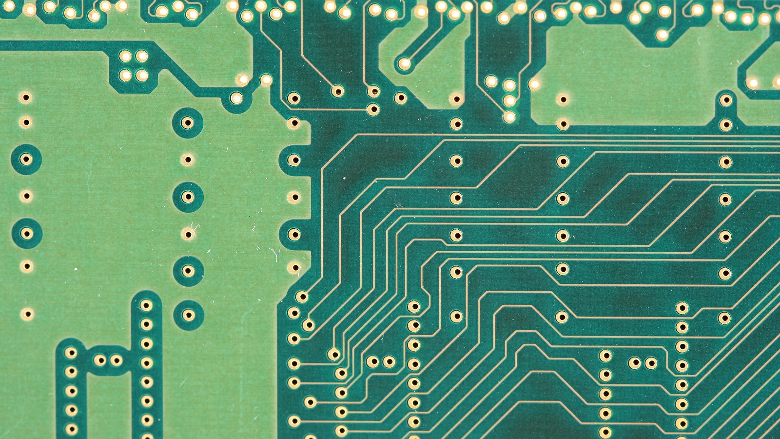
Step 7: Add Drill Holes
Define where drill holes and vias will be on the board:
Drill Holes and Vias: Place these based on your design and mechanical requirements. Modify them as needed while routing.
Step 8: Route Traces
Connect components electrically by routing traces:
Routing Strategy: Critical connections like power, ground, and high-speed nets must be given priority.
Routing Tools: CAD tool advanced routing features can be used to draw traces quickly, while following all the design rules. Automatic routing is possible to speed up this step if the number of connections is large.
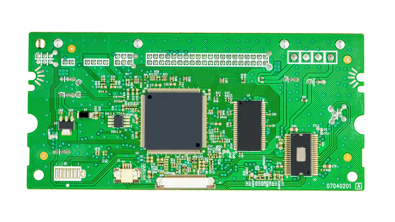
Step 9: Adding Labels and Identifiers
Label your PCB. This will help in assembling and testing:
Reference Designators: Put these in if you need to know which component is which when assembly.
Other Markings: Add polarity indicators, pin one identifiers, logos, part numbers as needed
Silkscreen Layer: Put all labels and markings into the correct overlay layers.
Step 10: Generate Design Output Files
Generate the files that will be used by the manufacturer for the board.
Run a final Design Rule Check: This is the last check for errors.
Generate Gerber Files: Generate Gerber files, Bill of Materials, and drill files (if required) for fabrication. These should include all information and instructions that are to be conveyed to the manufacturer.
Final Steps: Fabrication and Assembly
Fabrication
Send Files: Send your final files to the PCB fabrication facility.
Board Production: The facility will create a bare PCB, which etches traces and creates a layer stackup.
Assembly
Component Placement and Soldering: The assembly facility places the components on the board in their respective positions, following soldering.
Test and Inspect: The assembled PCB is tested comprehensively and inspected to ascertain the conformance of the board to design specifications and its operability according to stipulated needs.
Using these ten steps, you will be able to work through a process of PCB design in a manner where all phases are properly addressed and integrated. The orderly approach allows you to minimize errors, enhance functionality, and ensure manufacturability toward a final product.
Hot Tags:

Contact us

If you can't find what you're looking for, please contact us.
Article
PCBs (Printed Circuit Boards) are fundamental in electronics, composed of multiple layers like silkscreen, soldermask, copper, and substrate, chosen for specific electrical functions.
 2024/08/07
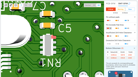
The article is developed concerning the breakthrough of integrated circuits and the need for custom PCBs in some electronic products. It enumerates ten golden rules in conducting PCB layout design and manufacturing: grid selection, routing, power layers, component placement, panel duplication, component value combination, frequent DRC, flexible silkscreen use, decoupling capacitors, and pre-production parameter checks. These rules provide for the optimum design and manufacturing of a PCB.
2024/07/25
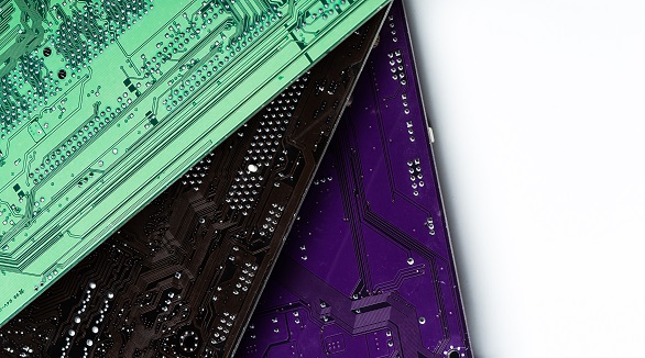
Most electronic circuits are mounted on PCBs, or Printed Circuit Boards, which provide mechanical support and electrical interconnection of electronic components. There are, however, special applications that involve the use of single and double-sided PCBs, multi-layer PCBs, or even rigid and flexible PCBs with aluminum backing, targeting medical, industrial, auto, and aerospace industries. They may use materials such as fiberglass, epoxy, aluminum, and others.
2024/07/25