- Products & Capabilities

- About
- Resources
How to Design a PCB Layout?


PCB layout design transforms schematics into reliable, efficient electronic products by optimizing signal integrity, power distribution, and thermal management.
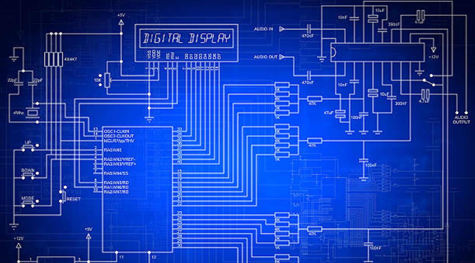
Printed Circuit Board (PCB) layout design is a sophisticated art, required for transforming a circuit schematic into a functional electronic product. Efficiently done PCB layout not only gives signal and power integrity but also optimizes electromagnetic compatibility, thermal equilibrium, manufacturability, and product reliability. We at PCBX are committed to leading you through this sophisticated process in a straightforward step-by-step approach in designing an efficient PCB layout.
Layout Planning and Stackup Design
Hardware Layout
The planning process starts with carefully thinking through the board architecture and selecting the layer stackup:
PCB Specifications: Understand board size, layer count, and estimated component density.
Schematic Review: Understand component types, quantities, and requirements.
Section Partitioning: Define analog and digital sections to minimize interference.
Interface Planning: Plan high-speed routing requirements.
Power Architecture: Develop a decoupling plan suitable for application.
Cooling Requirements: Identify which pieces must be thermally controlled.
Enclosure and Assembly Restrictions: Confirm physical design compatibility with intended housing and assembly processes.
Critical Nets Identification: Identify the critical nets for impedance control.
Guidelines for Routing: Adhere to standards of organizations like IPC.

Layer Stackup Definition
Layer Number Selection: Select an appropriate number of layers depending on board complexity and density.
Material Selection: Select dielectric material in order to best optimize performance parameters.
Copper Weights: Select suitable thicknesses to handle current loads.
Plane Layer Assignment: Save layers for power and ground.
Signal Routing Optimization: Route signal layers with optimized routing as the consideration.
Thermal Management: Use internal thermal vias or layers when necessary.
Thoughtful planning and stackup design form the foundation of successful sub-system integration and layout efficiency.
Component Placement
Proper placement of components is essential for successful PCB design:
Circuit Grouping: Bunch similar circuits near each other.
Critical Path Minimization: Shorten critical paths for key signals.
High-Speed IC Placement: Locate near connectors to maintain signal integrity.
Heat Source Distribution: Avoid hotspots by distributing heat-generating components.
Test Point Accessibility: Allow easy access for testing and debugging.
Component Orientation: Fix orientation for ease of assembly.
Placement Zones: Define clear zones for different design segments.
Right placement of components minimizes interconnect lengths, de-couples noise, and addresses potential thermal issues, and also caters to assembly needs.
Signal Trace Routing
Once components are placed, signal interconnect routing is of concern:
Correct Trace Widths: Use widths appropriate for current requirements.
Minimizing Critical Signal Paths: Keep these paths short to preserve signal quality.
Prevent Sharp Angles: Replace 90° angles with 45° bends for improved manufacturability.
Noise Isolation: Route sensitive signals away from noisy components.
Impedance Matching: Use techniques where there are high-speed signals.
Test Probe Accessibility: Allow for easy testing by providing paths.
Smart routing enables impedance control, minimizes electromagnetic interference (EMI), and ensures robust signal integrity.
Power Distribution and Decoupling
Proper power distribution is essential to circuit performance:
Power/Ground Planes: Use large planes for good current distribution.
Bypass Capacitor Placement: Locate close to ICs to prevent inductance.
Local Via Usage: Route devices directly over the power plane.
A solid power distribution network and decoupling techniques in combination provide stable supply voltages, ensuring reliable operation.
Thermal Management
Good thermal management practices must be implemented to ensure longevity:
Component Identification: Determine what components require heat sinks based on power dissipation.
Thermal Via and Pad Use: Provide enhanced heat dissipation from the component.
Airflow Management: Position components to allow proper airflow over heat sinks and vents.
Addressing thermal considerations guarantees long-term functionality by effectively dissipating heat from critical components.
Mechanical Features
Incorporating mechanical features completes the design:
Mounting Provisions: Offer holes and connectors for structural integrity.
Indicators and Test Points: Enable usability and test points.
Component Marking: Offer clear identification for assembly precision.
These capabilities aid in physical assembly, enable testability, and confirm correct application of the PCB.
Finalizing Layer Stack
Routing complete, finalize your layer configurations:
Review Routing: Ensure optimal use of layers and work out issues discovered.
Spacing Violation Checks: Check against fabrication limitations.
Layer Alignment: Ensure precision with reference markers and test points.
Finalizing the layer stack integrates all elements into a cohesive design, ready for production.
Design Rule Checks
Conduct careful design rule checks to ensure compliance:
Electrical and Routing Rules: Confirm clearances by voltage levels.
Manufacturing Rule Compliance: Confirm compliance with the ability to fabricate.
Using automated tools guarantees the design is solid and ready for manufacture.
DFx Analysis
Rigorous DFx analysis ensures the design meets functional requirements:
Signal Integrity: Check crosstalk and reflection issues.
Power Integrity: Ensure power network integrity.
Thermal and EMI Testing: Test to identify potential hot spots and emissions concerns.
Mechanical Stress Analysis: Test the physical durability of the design.
DFx analysis confirms the PCB design's ability to withstand operating loads and industry requirements.
Layout Optimization
Iterate on feedback to refine the layout:
Trace Adjustments: Correct width and spacing mistakes that impact performance.
Trace Adjustments: Correct widths and spacing issues impacting performance.
Thermal Improvements: Optimize heat dissipation paths.
EMI/EMC Revisions: Redirect signals to minimize interference.
Iterative optimization provides a very optimized design that meets electrical, thermal, and mechanical requirements.
PCB layout design is an exacting task involving diligence, meticulous planning, correct routing, and strategic parts placement to optimize signal integrity, power distribution, and heat management. By following best practices and with the use of advanced validation tools, designers can create stable, production-ready PCBs with improved performance and longevity. We at PCBX endorse a systematic approach to PCB design, enabling innovation and technological advancements in all electronic endeavors.
Hot Tags:

Contact us

If you can't find what you're looking for, please contact us.
Article
PCB schematics map circuit connections, while layouts focus on physical design for manufacturing. Both stages ensure optimal and reliable PCB design.
 2025/02/11
PCB design trends include miniaturization, advanced materials, sustainability, automation, and security, aligning with technological advances and diverse industry demands.
2024/10/22
High-speed PCBs (>1GHz) are crucial for advanced electronics like 5G and data processors. Key practices include ensuring signal integrity, controlling EMI, and maintaining power integrity for reliable performance.
2024/09/27