- Products & Capabilities

- About
- Resources
How to Repair PCB Traces?


PCB traces, vital for electrical connectivity, can suffer from stress, corrosion, or heat damage, and are repaired by careful inspection, cleaning, and soldering.
Printed Circuit Boards (PCBs) are the backbone of modern electronic technology, allowing the easy transmission of electrical signals through copper paths etched out on the circuit board. The copper paths play a critical role, as they connect various components in electronic devices from simple gadgets like smartphones to advanced manufacturing machines. Still, the copper paths on the PCB face the threat of damage. Physical damage, corrosion, exposure to high temperatures, and design flaws can affect the usability of the copper paths, resulting in the malfunction of the affected electronic devices. However, the view that you can never revive a defective PCB is untrue, as there exist workable solutions to revive the copper paths and save you money and electronic devices from the junkyard known as the world of e-waste. This tutorial will help you to learn step-by-step procedures to revive the copper paths on the defective PCB.
Importance of PCB Traces and Factors that Cause Damage
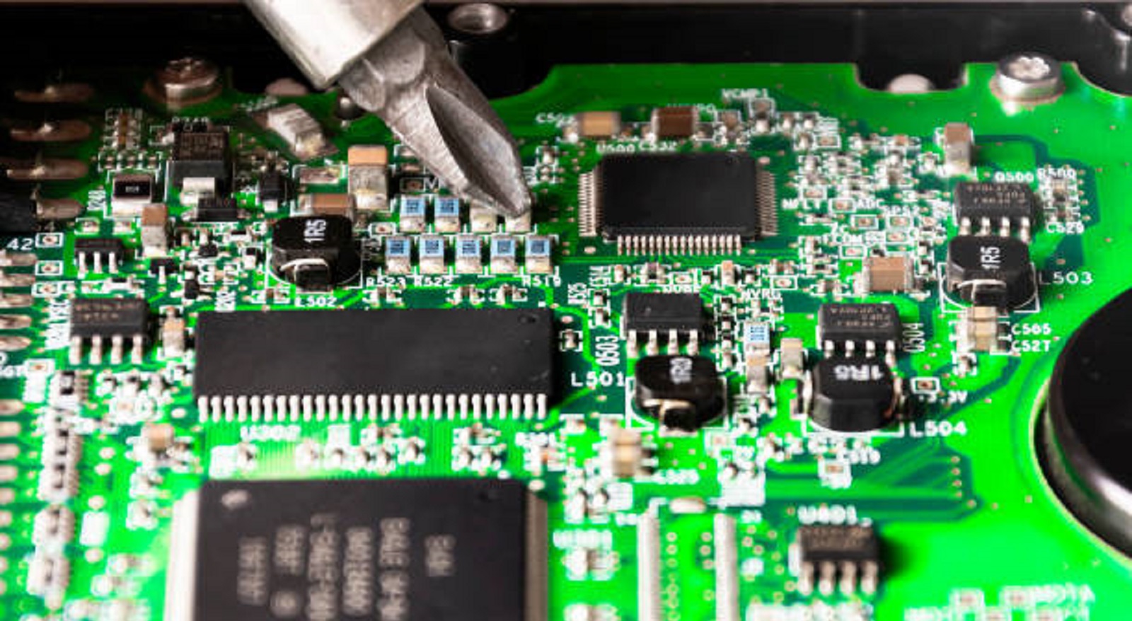
PCB traces consist of thin strips of copper material etched on the board surface. They act as very important tracks for the flow of electric signals; they are like highways for vehicles. Any form of damage may result in the inhibition of the flow of signals and subsequently cause device malfunctioning.
Physical Stress: Mishandling, such as dropping the components and using too much force when connecting them, can cause pathways to break. For example, when connecting the plug to the board, the pathways can be stressed or broken.
Corrosion: While copper may corrode due to the effects of moisture and chemicals, this could react with the copper, increasing the resistance of the copper, thus causing impaired connections. One leaking capacitor could result in dripping chemicals on the copper, hence intensifying the problem.
Overheating: Extended exposure to high temperatures—frequent in heavy soldering operations or high-current applications—is another common cause of trace lifting, burning, or other defects on sensitive substrate types such as FR4.
Design Mistakes: A narrow trace width might cause overheating of the traces, where high currents are involved. For instance, in the case of a circuit with 2 amps, where a narrow trace was used, thermal stress and eventual failure might be experienced.
Essential Tools and Materials for PCB Repair
The right kind of tools and materials should first be equipped to carry out repairs on the PCBs effectively and accurately:
Soldering Iron and Solder: The soldering iron should be temperature controlled with a fine tip for good accuracy. Use rosin-core solder since it allows for the best adhesion and clean joints.
Multimeter: This is a very important tool in determining the extent of the damage through the measurement of continuity and testing whether the repair was successful.
Conductive Ink Pen: A great tool for simple trace crack repair. Conductive ink is a silver-based ink that provides a low resistance method of connecting interrupted paths.
Jumper Wires: These may be required if there is no direct path on which you can jump your connections; thus, jumper wires will help you
Copper Tape: A solution with adhesive that can be utilized to replace parts of or an entire trace that is missing or severely damaged.
Desoldering Tools: It is important to use braids or pumps when desoldering as they are helpful in removing unwanted solder and also create a clean environment around the
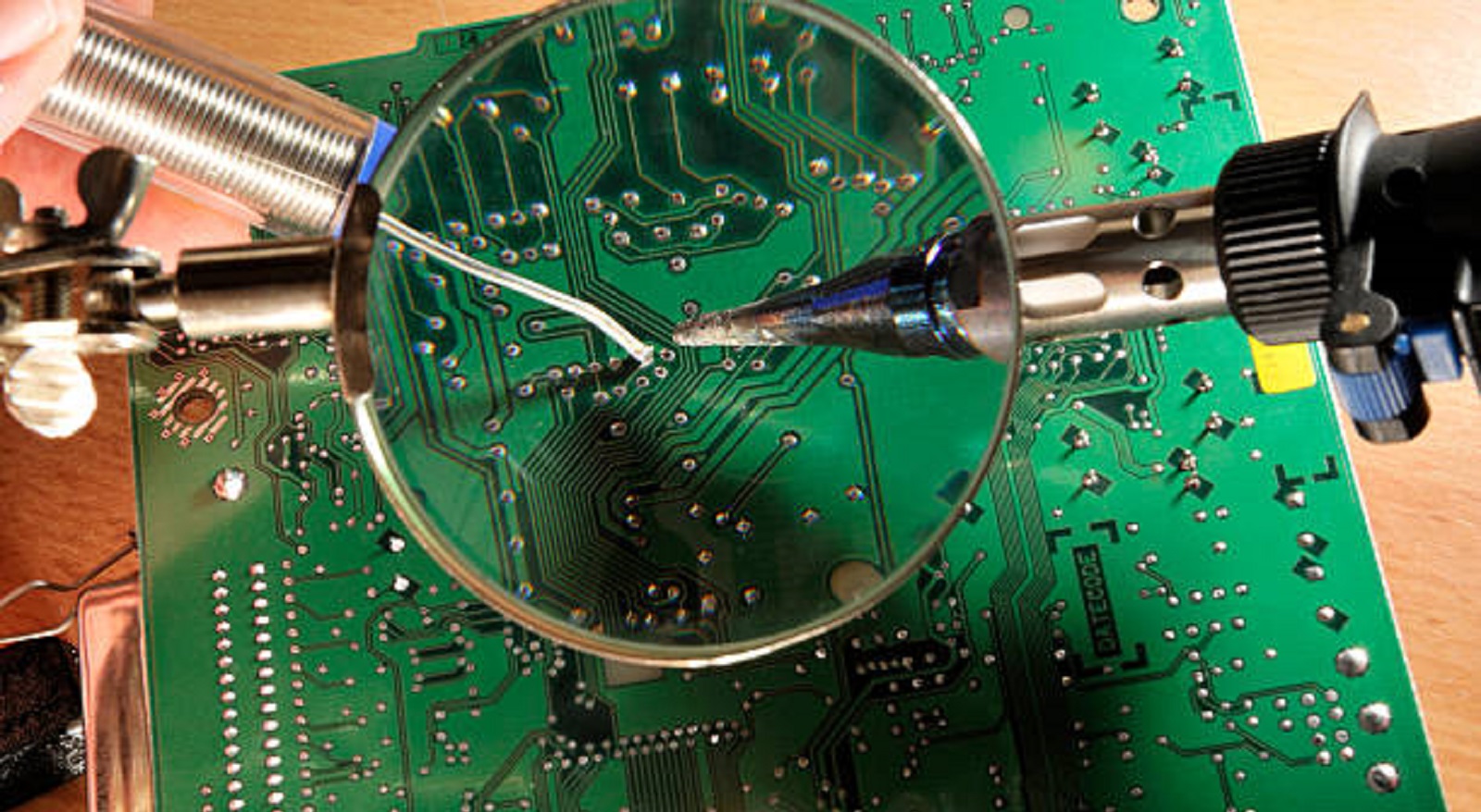
Magnification Tools: A magnifying glass or a microscope can be used to inspect complex tracing features closely.
Cleaning and Protecting Supplies: The materials needed include isopropyl alcohol for cleaning, and UV cured solder mask or conformal coatings for environmental protection of completed repairs.
Step-by-Step PCB Trace Repair
Identify the Damage:
Visually inspect under proper lighting and magnification if necessary, checking for cracks, breaks, or corrosive areas.
Check suspected damages with multimeter in continuity mode. An open circuit (no continuity) confirms a trace disruption.
Prepare the Working Area:
Thoroughly clean the corroded area with isopropyl alcohol to eliminate debris, dust, and other pieces of corrosion that may still be present. Ensure that no dampness remains on the surface.
Select and Implement a Repair Strategy:
Minor Damage: In cases of minor cracks or breaks, clean over the damage with a conductive ink pen. Ensure the ink overlaps intact copper for full restoration of the path.
Severe Breaks: If the gap is large and the trace is missing, use jumper wires or copper tape. Heat and carefully solder jumper wires across the gap, using copper tape with its ends soldered down to keep things in place. Make sure that the width and thickness of the wire or tape are adequate to carry any current that the trace was intended for.
Secure the Repairs:
Apply flux to the area to be soldered to help the flow of the solder and to increase the strength of the connection.
Use heat to the least amount necessary to prevent further damage. Thus, quick accuracy prevents lifting or damage to adjacent structures.
Use Kapton tape or epoxy for stabilizing repairs so that positional integrity can be preserved.
Validate the Repair:
You will use the multimeter to test whether there is now constant current flow through the fixed areas. A resistance value below 1 Ω should demonstrate that the repair has been successful.
Protect and Insulate:
Add a UV curable solder mask or conformal coating on top of your repaired trace in order to add a protective layer against moisture, dust, or physical wear and tear.
Best Practices for Successful PCB Repair
Emphasis on Precision: Work with tools and parts cautiously, with every step carried out with emphasis on high precision.
Safety and Preparation: This project always has to be done in a static-free environment using anti-static wrist straps.
Skill Building: Work on practicing your repair skills on some scrap boards before you work on critical repairs.
Detailed Documentation: Keep detailed documentation of each repair that can be utilized later, especially when repairing circuit boards.
Thermal Management: The proper use of solder temperatures and time to reduce thermal stresses to sensitive devices.
The ability to repair PCB traces is a skill set that can be very useful for both hobbyists as well as professionals, as this skill can save them time, money, as well as preserve the functionality of their electronic devices. The key to fixing a PCB trace—whether at a professional level or for a personal project—is to understand the nature of trace damage, use the appropriate tools, and follow a step-by-step process. Do not be intimidated by the process, as the skill can be very rewarding, especially if you're able to revive a malfunctioning piece of technology.
Hot Tags:

Contact us

If you can't find what you're looking for, please contact us.
Article
PCBs are essential but prone to faults. Diagnosis and repair using tools like multimeters and X-rays prevent costly repairs, ensure reliability, and improve quality.
 2024/11/26
PCB repair skills reduce waste and costs, ensuring durable electronic functionality by effectively diagnosing and fixing various board failures.
2024/10/25
PCB trace technology is crucial for modern electronics, ensuring reliable and efficient signal transmission. Key elements include trace width, spacing, and material selection.
2024/09/25