- Products & Capabilities

- About
- Resources
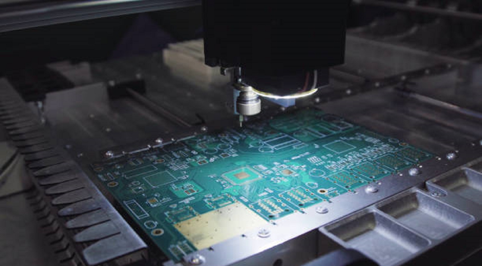
Laser Print PCB


Laser tech revolutionizes PCB manufacturing with precision and efficiency, enhancing design, cutting, marking, and connectivity while reducing environmental impact.
In the fast-moving world of electronics, Printed Circuit Boards, or PCBs, form the indispensable base on which intricate electrical devices are built. As technology advances, so do the means of making printed circuit boards, and laser technology is one such important development. Laser system integration contributed to an outstandingly perfect match for the fabrication industry of printed circuit boards. It is about the combination of accuracy, productivity, and novelty.
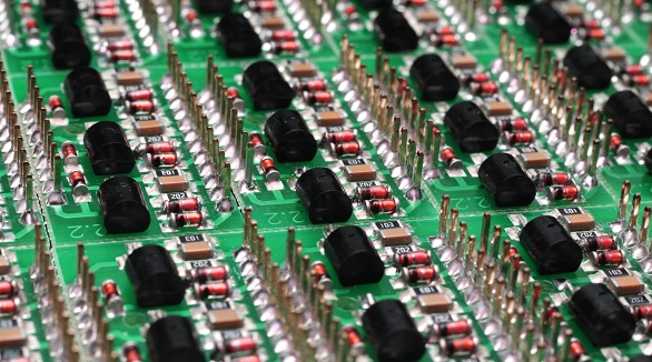
The process of manufacturing PCBs is a very complex procedure, involving many stages that need highly specialized tools and engineering skills. These traditional processes have remained basically tied to chemical etching and other manual interventions, which have been long, laborious, and costly despite their effectiveness.
Lasers have revolutionized this landscape, offering a whole raft of benefits at different stages of production. It has opened a whole new era in the creation and design of PCBs since laser technology obviates much of the limiting factors associated with traditional manufacturing.
Materials and Design: The Building Blocks of PCBs
Material selection is the first step for any PCB fabrication and decides the electrical performance and mechanical reliability of the board. An engineer will select materials such as FR-4, ceramic, and flexible substrates for a circuit based on the intended application and operational environment.
Modern laser systems enhance this choice by allowing finer material handling and manipulation in the production process. For example, laser engraving provides an effective method of accurately shaping the material and laying out circuitry for optimal performance and durability. In designing complex circuit paths that are needed by advanced electronics, for instance, the degree of accuracy achievable is so much greater and with less chance of error during manufacturing.
Laser Marking: Precise Identification
Accurate marking of components and circuits is an important part of PCB manufacturing. Identification markers on the PCB facilitate identification and, hence, connectivity, making the entire process integral to assembling and maintenance of electronic devices. Earlier, alphanumeric markings were done by manufacturers; however, such marking faces its limitations in the compactness of a PCB with small surface area.
This challenge overcomes with the advent of laser marking technology, which allows for advanced engravings of complicated identifiers, such as barcodes and QR codes, capable of carrying a big chunk of information in very little space. In such a laser-driven marking process, readability is clear and precise, performance is stable over time, without causing any harm to the PCB surface. Besides, laser marking enables the possibility of fast and efficient labeling-pretty important for high-volume production environments.
Laser Cutting: Revolutionizing PCB Fabrication
Probably, the most impressive intervention of laser technology in making PCBs relates to cutting. Laser cutting allows a high degree of precision and cleanliness without actual physical contact with the PCB material. This no-touch method minimizes stresses on the board, reduces material waste, and keeps the structural integrity of the substrate intact.
With much speed and precision, fiber laser systems work effectively for the cutting of stencils in PCBs. The laser beam can create minute patterns and shapes needed for the complex layout of circuitry, optimizing the manufacturing process in this respect. Another benefit of non-contact laser depaneling-separated individual circuit boards from a greater panel-is the protection of sensitive components and solder joints to make sure each cut is both accurate and aligned.
Laser Sintering: New Frontiers of Interconnectivity
Laser sintering is a major development that overcomes many problems of traditional soldering. It heats up the conductive materials on the PCB by using a laser in very select areas, forming much stronger and reliable connections. Moving away from conventional soldering techniques, laser sintering offers greater stability of the joint and is very useful in high-density PCBs.
The process generally includes exposing a laser to a powder containing silver, which causes heat to the melting point of powder. After it cools, it becomes one strong conductive path. All this can become advantageous in ensuring better durability and connectivity, giving designers more possibilities for next-generation electronic devices.
Laser Drilling: Precision in Layer Connectivity
In most of the cases, PCBs have to use inter-layer connections in order to embed different components in a compact footprint. Laser drilling offers unparalleled levels of precision and control, allowing manufacturers to make micro vias and interconnects essential in modern multi-layered designs.
Unlike traditional mechanical drilling, laser drilling is a non-contact process that ensures vibrations cannot affect the structural integrity of the material. This capability is especially important when drilling small-diameter vias, which demand a high aspect ratio, specifically, the balance between the diameter and depth of the hole. The laser can provide very precise control over beam intensity, duration, and heat emission, making for very high-quality repetition in each and every hole drilled.
Selection of the Proper Laser in PCB Applications
Different laser systems offer a unique advantage when related to manufacturing requirements. UV and CO2 lasers are used in different applications of PCB production. With UV lasers, 'cold' cutting occurs, with much less damage to the thermal edge surfaces, so they find applications in areas where material integrity is critical. However, they usually have a greater cost and slower processing speeds.
Whereas, in contrast, CO2 lasers are much more effective for applications requiring faster cutting cycles and thicker substrates. These are the cost-effective ones but may provide more charring and a wider cut width. These factors need to be balanced by the manufacturer while choosing the laser source for a particular PCB application.
The Future of Laser-Enhanced PCBs
Laser technology brings a whole revolution in manufacturing to PCBs, with perfect precision, efficiency, and flexibility. With the introduction of laser-printed PCBs, production processes can now fulfill even higher complication in design specifications and quick responses toward market requirements.
Lasers in modern PCB manufacturing are not only a tool but a force bringing down environmental impacts and increasing the capacity of electronic products. With ever-improving technologies, the place of lasers within PCB production would also be widening further, propelling the making of new thresholds for quality and performance within this industry. As improvements are on track continuously, laser technology should also make serious alterations in electronics manufacturing-a complete era of preciseness and reliability.
Hot Tags:

Contact us

If you can't find what you're looking for, please contact us.
Article
Burn-in boards are vital for testing semiconductor reliability, simulating stress to reveal defects, ensuring high-quality devices before mass production.
 2024/12/06
Carrier PCBs are crucial for data modulation, multiplexing, and network integration, supporting efficient and robust telecom infrastructures globally.
2024/12/06
Amplifier PCBs enhance audio signals in devices like headphones and theater systems using components like transistors and capacitors for clear sound.
2024/11/22