- Products & Capabilities

- About
- Resources
Navigating the Complexities of 01005 Component Assembly


01005 components are key for miniaturization in electronics, requiring precise handling in PCB assembly to overcome challenges in soldering, placement, and inspection.
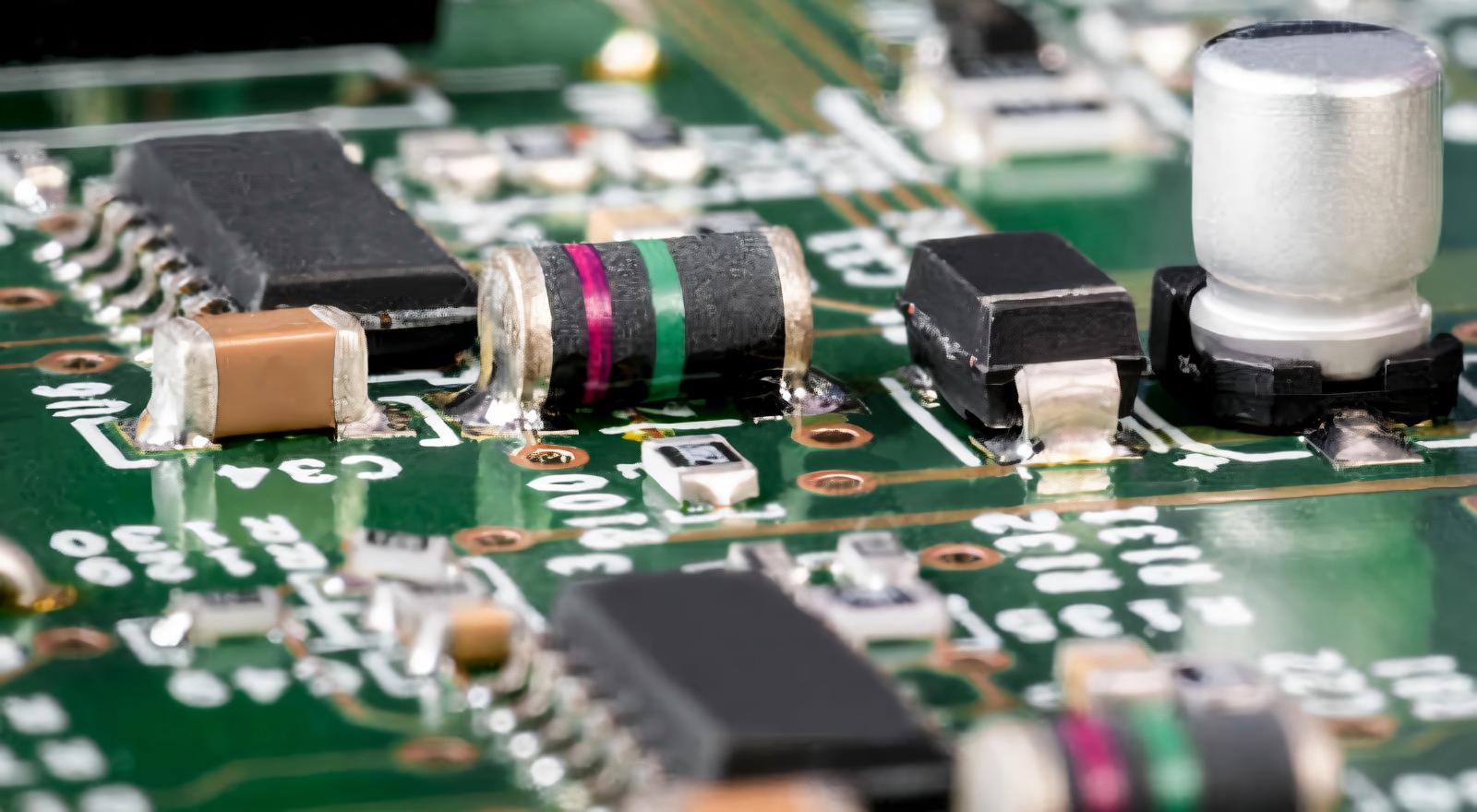
Miniaturization is a driving force for the innovation that is happening on the electronic frontier, and it challenges the engineering community to rethink the process of printed circuit board (PCB) assembly. Among the most complex technologies involved in this shift is the 01005 passive device, which is the smallest component measuring 0.4 mm x 0.2 mm. Despite the size constraint associated with the component, the 01005 device plays a pivotal role in the design of highly compact devices such as smartwatches, IoT devices, and smartphones. Interestingly, despite the immense benefits associated with the component, the process associated with handling and assembling the component on the PCB is even more complex and challenging. This piece explores the challenges associated with the assembly process and how to achieve success.
The Fundamental Nature of 01005 Components
The 01005 components are on the cutting edge of miniaturized electronics, functioning as an essential element within applications when high-density layouts are required. The size factor allows it to mesh well between pins on compact Ball Grid Arrays. In addition to their high-tech applications, compact devices require these components to have key functions such as signal processing or decoupling capabilities. However, to implement them, it requires an understanding of their assembly.
Critical Challenges and Solutions in 01005 Assembly
This is from a series of challenges identified in the literature review.
Challenge 1: Accuracy in Solder Paste Printing
Solder paste printing is typically the first and most critical process in assembly. The minute size of the 01005 pads requires a very high level of accuracy for correct solder deposition.
Solutions:
Advanced Stencil Technology: The employment of high-quality stencils, including electroformed or laser-cut stencils, is paramount. These stencils should feature well-defined apertures, which could optimize the paste transfer by reducing the variability and ensuring a well-balanced solder distribution.
Process Parameter Optimization: Refine printing parameters like speed and pressure while incorporating automated optical inspection to perform the process in real time. Consistent application is very crucial in avoiding defects arising from uneven paste deposits.
Challenge 2: Component Placement Accuracy
Due to the level of accuracy required in handling 01005 components, placement methods prove to be inadequate in some manner, potentially resulting in alignment issues.
Solutions:
High-end Placement Equipment: Invest in high-end pick and place equipment that also incorporates high-end vision systems. This will improve the accuracy of the placements. The equipment will be designed to handle the size and fragility of the 01005 devices.
Dynamic Process Adaptation: Use machine learning algorithms for adapting placement processes that improve accuracy and minimize the chances of human errors.
Challenge 3: Controlled Reflow Soldering
Reflow soldering of 01005 devices can be problematic due to the thermal sensitivity of such a small device. Error here can cause the defects of tombstoning or bridging.
Solutions:
Precision Thermal Profiling: Create reflow profiles that address process issues based on the known properties of 01005 devices to provide uniform heat distribution and controlled ramp to prevent component migration during reflow when melting solders.
Continuous Monitoring Systems: Real-time thermal monitoring can be implemented for adaptive control of the reflow process based on the temperatures for a reliable solder joint.
Changing 4: Successful Inspection & Quality & Control
The inspection of 01005 component packages is very complex because of their small size and challenges the limits of conventional automation for inspection.
Solutions:
Hybrid Inspection Methods: It can be done by integrating AOI systems with a high-resolution imaging process along with a verification process by humans for critical areas. It ensures that there is accurate identification of defects.
Innovative Imaging Solutions: Use advanced imaging solutions that are able to distinguish between real flaws and false notifications, thus enhancing the effectiveness of the defect detection process.
Challenge 5: Overcoming Rework and Repair Challenges
Being the smallest in size and having a dense packing pattern, the task of reworking 01005 components is a challenge.
Solutions:
Proactive Defect Mitigation: Emphasizing a strong first pass yield through upfront design optimization and upfront testing to limit rework.
Precision Rework Tools: Utilize advance rework tools that allow heating control and optical guidance, ensuring that the rework process done is precise and does not damage neighboring components.
At PCBX, we respond to the challenges of 01005 component assembly with innovation and experience. Our modern facilities feature the most up-to-date SMT technology, along with multi-zone reflow ovens for precision in the placement of these minuscule components. With our rapid prototyping, we can hasten the cycles of design iteration and optimization. We have a fully guarded supply chain to ensure timely delivery of all components. With strict adherence to the principles of DFMA and IPC standards, we guarantee first-class quality.
To successfully assemble 01005 components in PCBs, there must be a holistic way of tackling design, technology, and process improvements. Through investments in highly advanced manufacturing equipment, improvements at every step of the process, or by collaborating with experts, the potential of these components can be realized. Such efforts will enable the production of more complex, compact, and highly advanced electronic products. At PCBX, we are ready to help make this possible by assisting our partners in tackling the difficulties associated with advanced electronics assembly.
Hot Tags:

Contact us

If you can't find what you're looking for, please contact us.
Article
ARM processors are efficient and flexible, ideal for many applications, while FPGAs offer custom parallel processing, crucial for specialized tasks requiring flexibility.
 2025/01/21
SMA connectors are cost-effective for up to 18 GHz, while SMC excels beyond 26 GHz. Each suits different needs in RF/microwave applications, depending on budget and specs.
2024/12/12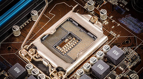
FPGAs offer high flexibility and capacity for complex designs, while CPLDs provide simplicity and cost-effectiveness for smaller applications, crucial in PCBs.
2024/11/20