- Products & Capabilities

- About
- Resources
PCB Lamination Process


Learn how the PCB lamination process uses thermal curing and dielectric prepreg to bond multilayer boards for superior electrical and structural integrity.
PCB lamination is the process through which circuitry layers of copper and insulating materials have a controlled bonding process of these two layers at pressure and heat to create just one board. However, in practice it is a very engineered thermal and mechanical process which has a direct impact on electrical performance, structural integrity and manufacturing lead time.
What Is PCB Lamination and Why It Matters
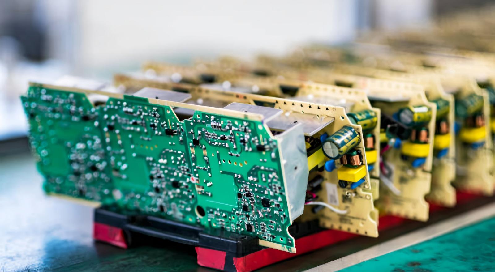
Multilayer PCBs have internal copper layers and are used in telecommunications equipment, medical equipment, automotive electronics, and industrial control systems. Such internal circuits have to be bonded together permanently with accurate dielectric spacing and mechanical stability.
PCB lamination attains three fundamental goals:
Electrical Connectivity: Provides the correct insulation between conductive layers and provides the correct dielectric thickness to control impedance.
Mechanical Strength: Provides a stiff, tough frame that can resist thermal cycling and mechanical forces.
Environmental Protection: Coats inner circuitry, moisture, contamination, and delaminations.
Since lamination lies at the heart of multilayer fabrication, any inefficiency or fault in this step propagates downstream operations, possibly increasing production by days.
Basic Materials in PCB Lamination
The lamination involves various engineered materials, which affect processing time and ultimate performance of the boards.
Copper Foil: The conductive circuitry is made of electro-deposited or rolled copper foil. Before lamination, surface treatment is essential in order to achieve high resin bonding.
Core Material: The core is usually fiberglass-reinforced epoxy laminate (usually FR-4). It offers structural stability and forms the foundation of internal circuitry.
Prepreg: Prepreg is partially impregnated resin-impregnated fiberglass. In the lamination process, the resin is then flowing liquid that fills micro-voids and then completely cures to unite layers. Curing time and temperature requirements are dictated by resin chemistry.
The choice of material has a direct impact on the lamination cycle time, particularly when using high-Tg, high-frequency, or specialty laminate.
PCB lamination Process
Inner Layer Preparation
Internally etched and inspected copper layers are then laminated. The inner layers undergo:
Pattern imaging and etching
Surface treatment (oxide or other bonding treatment)
Automated optical inspection (AOI)
Surface preparation improves the bond of resin and minimizes the chances of delamination. This phase may take a number of hours, per batch, depending on the complexity of the board.
Registration and Layer Stacking
Ready inner-layers are piled into a very specific order; prepreg sheets are interposed between copper layers.
The accuracy of alignment is important--particularly in multilayer designs with buried or blind vias. Compared to manual pin systems, automated optical alignment systems are much less susceptible to registration errors.
Stacking is comparatively easy with conventional multilayer boards (4-8 layers). In 12-16 layer boards, the cumulative tolerances make stack-up accuracy more complicated.
The wrong fitting at this point may result in open circuits or via breakout, and may need rework that will take 24 hours or more.
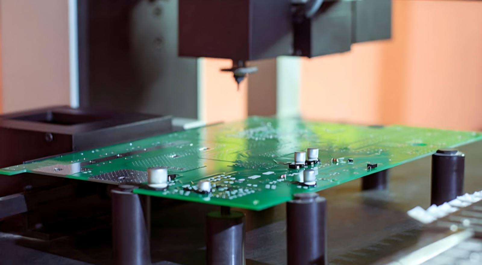
Lamination Press Cycle
The panel is stacked and placed in a hydraulic lamination press. Here, the individual layers are subjected to controlled temperature and pressure to create a solid composite structure.
Typical parameters include:
Temperature: 170℃-200℃
Pressure: 200-400 psi
Cycle Time: 1.5-3 hours
Lamination cycle consists of three regulated stages:
Heating ramp-up: The resin solidifies and starts to flow.
Gel and cure stage: Resin cross-links and hardens.
Pressure maintenance: Guarantees a vacuum-free bonding and consistency in thickness.
Thick boards or more layers take longer to heat and stay longer during dwell time because they have a greater thermal mass. Every new layer generally introduces a cycle time increment.
In sophisticated stack-ups, the two may be sequentially laminated, with repeated presses to form complex structures like HDI boards. This enhances reliability but it greatly increases the manufacturing time.
Controlled Cooling
Panels should be allowed to dry slowly under pressure after curing. Quick cooling may cause internal stress, warping or cracks in the resin.
The estimated time to cool is 1-2 hours, depending on the thickness and type of board used. This stage is very critical though not often considered, and is important to the question of dimensional stability.
Post-Lamination Inspection
Quality control includes:
Visual inspection
Thickness measurement
Internal voids X-ray
Peel strength testing
Early detection of problems avoids wastage of time in downstream drilling and plating. Nevertheless, when a flaw like delamination or voids is detected, it can be necessary to scrap boards, which would require 1-3 days on the production timeline.
Major Factors that Influence PCB Lamination Time
Material Selection
The behavior of resin systems varies greatly:
Normal FR-4 epoxy: Faster drying, usually 1.5-2 hours.
High-Tg materials: Longer curing time and elevated temperatures.
High-frequency laminates: Frequently have long dwell times and tight process control.
Advanced materials certainly enhance performance, but can also raise the lamination cycle time by 20-50%.
Temperature Control
Accurate thermal profiling is necessary.
If temperature is too low:
Under-curing of resin results in poor bonding.
If temperature is too high:
Too much resin flow can lead to voids or dielectric inconsistency.
Newer lamination presses with programmable heating patterns minimize defects and minimize the stabilization time.
Board Thickness and Count of Layers
A 4-layer PCB can be laminated within less than two hours.
A 12- or 16-layer board may take 3-4 hours or more.
High-density designs can require several lamination processes, doubling the overall processing time.
Equipment Capability
High vacuum lamination presses remove entrapped air and provide resin uniformity. Old machinery might need a more time to obtain the same quality, taking more time to produce.
Common Lamination Challenges
In spite of process controls, manufacturers should beware of:
Delamination: In many cases under-curing or contamination causes delamination.
Void formation: Voids form because of bad flow of the resin or entrapment of air.
Warping: Due to asymmetrical heating or material difference.
Resin starvation: Causes a variation in dielectric thickness.
To prevent setbacks during production, proactive monitoring and preventative maintenance are needed.
The PCB lamination is much more than a bonding process--it is the mechanical and electrical backbone of all multi-layered boards. Not only board quality but also manufacturing speed is determined by the selection of materials, the number of layers, press settings, and control over the cooling.
At PCBX, we view lamination as a precision engineering process where optimization directly translates into faster lead times and higher reliability. By carefully balancing material performance with thermal efficiency and equipment capability, we can streamline production while maintaining strict quality standards.
Hot Tags:

Contact us

If you can't find what you're looking for, please contact us.
Article
PCB edge plating enhances connectivity, mechanical strength, EMC, and thermal management, crucial for diverse sectors, with trends toward higher density and durability.
 2025/11/11
PCB printing services are crucial for transforming complex designs into efficient parts, offering precision, cost savings, and access to advanced technologies.
2025/02/05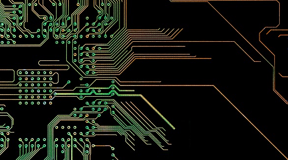
PCB trace technology is crucial for modern electronics, ensuring reliable and efficient signal transmission. Key elements include trace width, spacing, and material selection.
2024/09/25