- Products & Capabilities

- About
- Resources
What Is Automated Optical Inspection (AOI)?


AOI uses cameras and software to automatically inspect PCBs for defects, ensuring high quality, reducing costs, and improving reliability in modern PCB manufacturing.
With the further development of the electronic devices into the smaller sizes, the faster speed, and the more functionality, the complexity of the printed circuit boards (PCBs) has become more and more complicated. The layout of modern PCBs is sometimes dense, with fine-pitch packages and thousands of solder joints and the standard methods of manual inspection can be both inefficient and unreliable. To ensure quality production, PCB manufacturers use Automated Optical Inspection (AOI) - an important inspection method to be applied in the fabrication as well as assembling PCBs.
AOI is a critical part at PCBX to ensure that all boards assemble off the production line are of high quality, manufacturing defects are reduced as well as production costs are minimized. Knowledge of the AOI operation and its significance can be used to explain why it has gained commonality in the entire electronics sector.
What Is Automated Optical Inspection (AOI)?
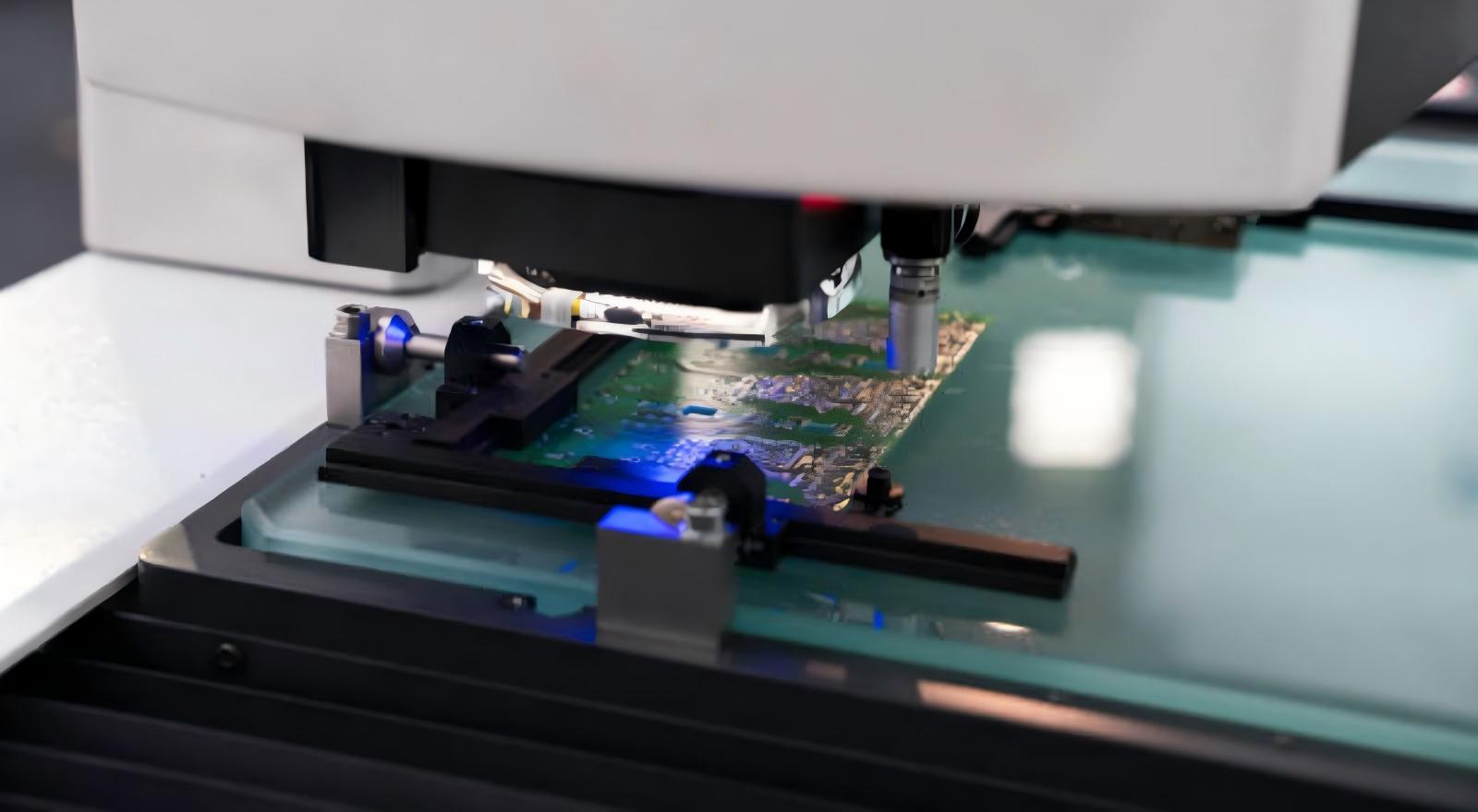
Automated Optical Inspection (AOI) is a machine-based visual method of inspection, based on high-resolution cameras, controlled lighting and image processing programs, to automatically scan PCBs to detect defects. It scans pictures of a circuit board and uses the result against reference information e.g. CAD design files or an established golden board to identify any deviation which may signal manufacturing issues.
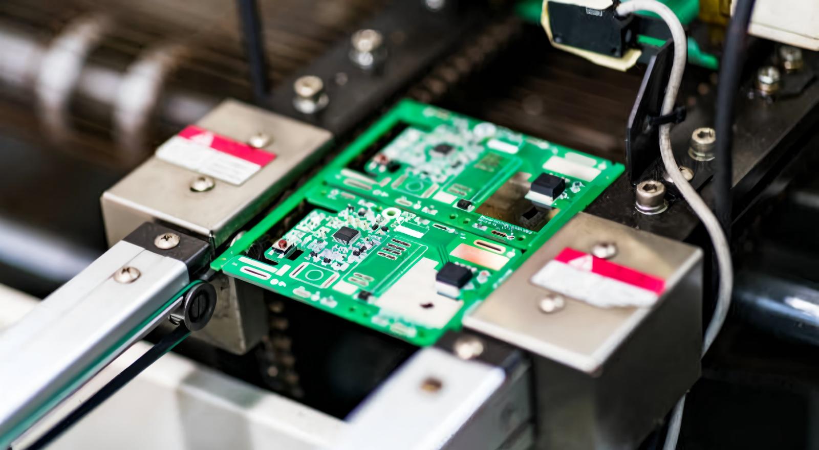
AOI is used at various production processes. It checks on structural integrity during PCB fabrication, such as trace patterns and pad integrity. In PCB assembly, it determines the position of components and the quality of solder joints once surface-mount or through-hole, which are checked.
During the more complex PCB designs the manual inspection is not able to accurately find small defects or even to maintain the quantity of production. AOI offers a quick, timely, economical inspection technique which can be utilized to ensure quality consistency in a large scale manufactured run.
How AOI Works?
AOI systems are machine vision and intelligent software systems that are used to conduct high precision automated inspections.
The machine starts with the entering of a PCB into the AOI machine through an automated conveyor. The scanned board has high-resolution cameras and captures detailed images of components, solder joints, pads, and circuit traces.
Lighting is very significant to accuracy of inspection. Current AOI systems incorporate adjustable programmable arrays of LED lights, turning the lights on and off depending on the angle and color of the light to increase contrast and display possible defects as well. The various lighting settings can be used to bring out certain problems like the solder bridges or misplacement of a component.
After taking pictures, they are examined by inspection software and shapes, dimensions, and positional accuracy are checked. The system will match the current images and reference data to detect the difference. The new generation AOI systems are able to make sub-pixel measurement accuracy which allows them to detect very small anomalies that would lead to electrical breakdowns.
In case of defects, the system leads the operator to their review, and captures data of inspection to facilitate the traceability and process improvement.
Application of AOI in PCB Manufacturing
Depending on the aims of inspection and cost-saving aspects, several stages of the manufacturing process can be incorporated with the AOI.
When bare PCBs are made, some of the AOI checks would be open circuity, short circuity, improper trace widths, spacing anomalies, or pad non-existence. These issues are identified at an early stage to avoid faulty boards getting into the assembly line.
AOI is usually employed in the PCB assembly lines before reflow soldering and after reflow. Pre-reflow checking is used to ensure that there is no solder past deposits and that the components are placed correctly. Post-reflow inspection is used to assess the quality of the solder joints and component positioning which is particularly necessary, as a lot of problems are caused during the soldering process.
AOI inspection is also conducted by some manufacturers prior to the shipment of products as a means of ensuring the overall quality of the products.
Defects Detected by AOI
The systems of AOI are programmed to detect a large variety of manufacturing and assembly mistakes in a brief span of time and with stability.
In the case of bare PCBs, short circuits, open circuits, a violation of line width or spacing, excessive copper, surface scratches, contamination, damaged vias or holes are some of the common problems that can be detected.
Through assembly inspection, AOI detects missing parts, wrong parts, polarity errors, misaligned parts, and skewed parts, flipped parts, and part placement errors. It also identifies the soldering defects which include inadequate solder, excessive solder, solder bridges, raised lead, tombstoning and inadequate solder coverage.
These issues can be detected early enough before the defective boards advance to the next stage of the production process where the cost of repairing the boards becomes very high.
Benefits of AOI in PCB Production
AOI has a number of significant benefits, which render it a must-have tool in the contemporary PCB fabrication.
The benefit of high standards of inspection is one. With the further reduction of components, even minute positional errors may result in failures. AOI systems are also capable of identifying small variations that are almost impossible to find through human hands.
AOI also lowers costs of manufacturing due to improved first-pass yield. Early identification of defects will save on rework, material waste and labor costs as production mistakes are avoided.
Flexibility is another benefit. AOI is able to check fabricated boards and assembled PCBs which is why it is applicable at several steps of the production process. Lighting is programmable and inspection parameters can be adjusted to fit various board designs and finishes.
Moreover, AOI systems gather data on inspections which are used in optimizing processes. Engineers are able to study the trends in defects, discover their root causes and optimize the manufacturing parameters to enhance the overall manufacturing efficiency.
The Reason AOI Is Gaining More and More Importance
The increased significance of AOI is also directly connected to PCB development. Fine-pitch components, high-density interconnect (HDI) designs and multilayer boards including complex boards and microvias demand greater precision in inspection than is possible by humans.
There can be thousands of solder joints on a single PCB and a defect rate that is even tiny can impact on the reliability of the product. Automated inspection brings about consistent quality with or without the scale of production and removes variances generated by fatigue or subjectivity of operators.
AOI also enhances the efficiency of manufacturing by making it possible to provide quick feedback. Identifying defects early in the process gives the engineers an opportunity to change the fabrication or assembly parameters in real time, so they do not cause the same problem to subsequent boards.
AOI and Complementary Inspection Methods
It is true that AOI is very effective in the detection of visible defects, but it is unable to check on the hidden connections underneath some component packages, say BGAs. To ensure quality, manufacturers usually use AOI together with X-ray inspection and electrical testing so as to verify internal solder joints and functionality of the circuit. The combination of these inspection techniques gives an overview of PCB quality.
At PCBX, AOI is stored in several important steps of fabrication and assembly processes to provide continuous and quality production. This enables manufacturing teams to control processes in real-time as well as easily detecting deviations, and exercising strict quality control during production, due to continuous inspection.
By integrating high-tech inspection with optimization, PCBX can deliver quality PCBs to our clients that can be used in harsh electronic tasks.
Hot Tags:

Contact us

If you can't find what you're looking for, please contact us.
Article
Superior PCBA testing ensures quality, functionality, and reliability, using diverse methods to prevent flaws, maintain standards, and enhance electronics manufacturing.
 2025/03/18
Surface Mount Technology revolutionizes electronics, offering size, cost, and performance benefits, but poses challenges with high setup costs and handling.
2024/11/04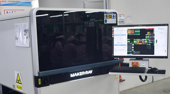
These SMT PCB assembly methods are involved, ensuring that several defects are detected. This includes the use of Automated Optical Inspection, In-Circuit Testing, and Automated X-ray Inspection. The combination of these methods is beneficial in facilitating an optimal inspection process.
2024/07/26