- Products & Capabilities

- About
- Resources
What is Chip-on-Board (COB) in PCB Design?


Learn what Chip-on-Board (COB) is in PCB design, covering types, manufacturing process, benefits and industrial applications for compact electronic circuit design.
Compared to the worldwide trend of miniaturisation, light weight and cost reduction, traditional prepackaged SMD chips are difficult to meet the requirements of compact layout and high heat dissipation of modern LED, wearable, automotive and medical electronics. Chip-on-Board (COB) is a type of electronics packaging that is considered to be in the intermediate stage of packaging, Level 1.5, and has become a mainstream specialized PCB assembly solution. Compared to conventional components that are packaged in plastic or ceramic packages, COB eliminates the need for individual chip packaging, thereby greatly reducing signal path length, maximizing thermal conductivity and conserving board space.
What is Chip-on-Board(COB)?
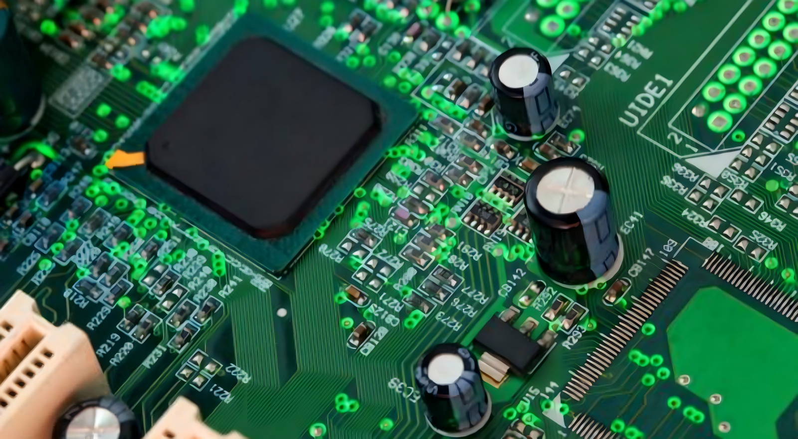
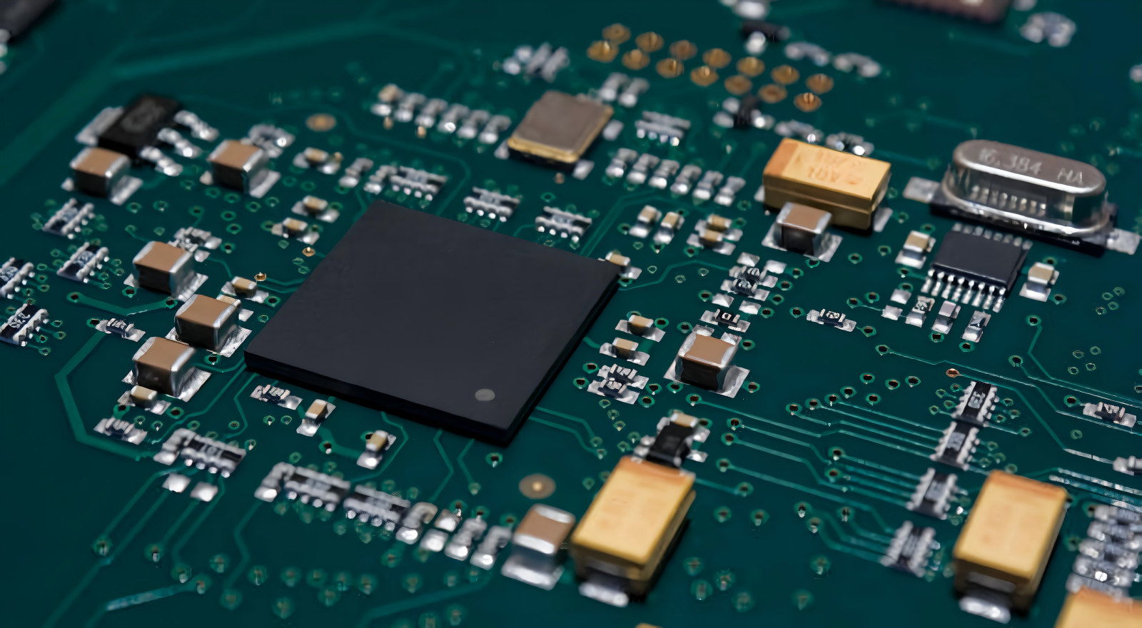
COB is a more advanced packaging technique which uses cured epoxy to completely encapsulate the chips and electrical connections to make stable electrical contact and to provide physical and chemical protection through fine bonding wires or flip-chip solder bumps, as well as pre-designed PCB bonding pads. COB reduces the amount of raw material waste as lead frames and separate packaging housings are eliminated, and can also reduce the total cost to about one-third that of the conventional packaged chip in mass production. There are two popular design formats for mature designs in use today:
Wire-bonding COB: The most common, a mature solution. The inner electrodes of the chips are then bonded to larger bonding pads on the PCB using ultra-fine gold or aluminum micro-wires via ultrasonic bonding, with bare dies glued to specific areas of the PCB. It is essential for PCB designers to carefully select and configure the size and pitch of the pads in accordance with the parameters in the die datasheet, otherwise it will easily cause a broken wire in the production process. All sensitive structures are protected against dust, moisture and mechanical damage by post-bonding epoxy glob-top.
Flip-Chip on Board (FCOB): Designed for high frequency and high density circuits. These are upside down, and have prefabricated solder bumps on the contact surfaces. The relevant PCB pads are treated with flux, and flipped chips are reflowed with the other passive components. Its PCB pad design is designed to conform to the modified BGA specification, specifying the bump dimension, which makes it possible to obtain ultra-short signal paths to minimize loss of high-frequency signals.
Seven-Step COB Manufacturing & Adhesive Selection
COB production is a set of seven standardized steps that meet the requirement of PCB design:
Substrate preparation: Thoroughly clean the PCB bonding regions and use a special surface plating on the designated regions to prevent cross-contamination in the assembly process.
Die attach: Automated pick and place tool is used to dispense selected adhesive and precisely position bare dies, with PCB leaving clear area for any overflow adhesive.
Pre-inspection: Ensure that the accuracy of the die is correct to avoid misplacing it.
Electrical bonding: Full bonding or full flip-chip reflow to ensure the stability of circuit connections.
Encapsulation: Over-coat chips and links with epoxy cured by UV or heat to create protective glob-top chips and links.
Multi-aspect testing: Run electrical continuity, visual inspection and temperature cycling tests to screen defective products.
Final assembly: Integrate qualified COB PCBs into finished electronic products.
There are two common adhesives used to attach the die: Silver conductive glue requires high temperature curing and is applicable to high power MCPCB that has high thermal dissipation requirements; Anaerobic glue is a type of glue that cures under anaerobic (airless) conditions, which are suitable for low power circuits that do not require thermal dissipation.
Important PCB Design Concepts for COB
There are a number of fundamental rules for COB reliability: First, the COB bonding pads are divided into separate blocks with larger copper sizes corresponding to the chip. Second, place dense thermal vias under high power dies to speed heat dissipation and prevent heat sensitive components from hot spots. Third, reduce the length of high-speed signal traces and include ground guard signal traces between analog and digital circuits to minimize the crosstalk and EMI effect. Fourth, provide sufficient air space between COB regions to provide for overflow epoxy during encapsulation. Last but not least, cover the bonding pads with hard gold plating and the rest of the circuit with cost-effective OSP/HASL for performance and cost.
Advantages and the Limitations of COB Technology
Benefits
COB consumes 30% to 60% less board area than traditional packaged chips in order to achieve the thinner device. Direct contact of the die to the substrate yields highest heat transfer and is dominant for high power LED modules. In mass production, the separation of the packaging is a significant cost reduction. A shorter connecting path reduces parasitic impedance for high-frequency electrical performance and full epoxy encapsulation provides protection from moisture, vibration and chemical erosion.
Drawbacks
The cost of small batch prototyping increases with specialized bonding equipment and design knowledge. After epoxying these faulty dies can't be replaced one by one – typically, a whole PCB has to be replaced, increasing the maintenance expense. Even so, passive components such as resistors continue to use the traditional SMT soldering, which restricts the whole board COB application.
Core Application Fields
The unique strengths of COB-equipped PCBs have resulted in their wide-spread market coverage in various industry segments. High power LED lighting is the biggest application scenario, and in this case, COB LED is also widely used in aluminum core MCPCB's commercial downlights, stage lighting and automotive headlight modules. COB is used in miniaturization of wearable electronics such as hearing aids and smartwatch control boards for reducing the thickness of the components inside the devices. COB's excellent anti-vibration and broad temperature flexibility are utilized in automotive electronics applications such as ambient light controllers in the car and tire pressure monitoring systems. COB PCB is also used in portable medical testing instruments and compact industrial signal transmitters in order to comply with the industry miniaturization and high reliability requirements.
COB is continually developing new products, technologies, and innovations to produce more fine-pitch flip-chip designs and optimized encapsulation solutions. While traditional SMD packaging still plays a dominant role in the majority of low-density circuits, COB is unmatched for high-power, miniaturized and high reliability electronic products in lighting, automotive, medical and new IoT fields. Electronic developers who need professional COB PCB layout validations, COB production and manufacturing feasibility consultant, PCBX delivers one-stop technical support covering PCB layout verification, substrate manufacturing and COB assembly feasibility assessment, helping electronic developers turn COB design concepts into stable mass-produced finished boards efficiently.
Hot Tags:

Contact us

If you can't find what you're looking for, please contact us.
Article
Step stencils optimize solder paste for varying component sizes in PCBs, enhancing reliability and reducing defects in complex designs with precision.
 2025/08/26
Ceramic Substrate PCBs boost innovation with superior heat management, strength, and miniaturization, making them vital in electronics across industries.
2024/10/30
PCBX offers fast, high-quality turn-key PCB prototype assembly services, including fabrication, component sourcing, and testing, all at competitive prices, to accelerate product development.
2024/08/14