
PCB Capability
PCBA Capability
Quality

PCB Capability
| Feature | Capability | illustration |
|---|---|---|
| Layers | 1-8 layers |  |
| Material | FR-4 |  |
| Board Thickness | 0.016"- 0.1"(0.4mm-2.5mm) |  |
| Outer Thickness | 1.0oz-2.0oz |  |
| Inner Copper Thickness | 0.5oz 1.0oz,2.0oz |  |
| Max Board Size | 500x600mm |  |
| Min Tracing/Spacing | 0.1mm(4mil) |  |
| Minimum Annular Ring | 0.125mm(5mil) |  |
| Min Drilling Hole Diameter | 0.2mm(8mil) | 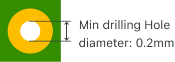 |
| Min Width of Cutout (NPTH) | 0.8mm | |
| Min Width of Slot Hole (PTH) | 0.6mm | |
| Solder Mask | LPI, different colors(Green, Black, White, Red, Yellow, Blue, Purple, Matt Black, Matt Green) |  |
| Silkscreen Color | White,Black |  |
| Surface Finish | HASL, Lead Free HASL, ENIG (1-3 micro inches), Immersion Tin, Immersion Silver, OSP |  |
| Max.Thickness of Au in ENIG | 2-5U" or >=5U" | |
| Surface/Hole Plating Thickness | 20-25um | |
| Board Thickness Tolerance | +/-0.1mm ~ +/-10% of thickness of board | |
| Board Size Tolerance | +/-0.1mm~+/-0.3mm | |
| PTH Hole Size Tolerance | +/.003*(+/0.08mm)~+/.006"(+/-0.15mm) | |
| NPTH Hole Size Tolerance | +/.002*(+/-0.05mm) | |
| Copper Thickness Tolerance | 0um ~ +20um | |
| SM Tolerance(LPI) | .003"(0.075mm) | |
| SMD Pitch | 0.2mm(8mil) | |
| BGA Pitch | 0.2mm(8mil) | 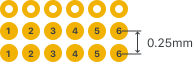 |
| Aspect Ratio | 1:8 (hole size:board thickness) | |
| Test | 10V-250V, flying probe or testing fixture | |
| Inspection Standard | IPC 2 IPC 3 | |
| Deliver Method | Single board without technical rail Single board with technical rail Panel with technical rail Others | |
| UL Marking | Marking of UL on board |  |
| Impedance Control | Impedance control tolerance:Regular impedance Control +-10% Non-Regular Control +-5% |  |
| Gold Fingers | Gold Fingers Chamfer:0° 20° 30° 45° 60° |  |
PCB
PCBA
Gerber File/PCB*.zip;*.rar;PCB
OR
Quantity