- Products & Capabilities

- About
- Resources
Anti-ESD Strategies for Reliable PCB Design


Practical anti-ESD strategies for PCB design, including layer stack-up, layout, routing, component use and testing.
Electrostatic Discharge (ESD) is a widespread menace to electronic equipment, and it is attributed to human contact, dry environmental conditions, as well as the equipment itself. This abrupt static charge transfer causes irreversible damage to the precision semiconductor, such as penetrating thin internal insulating layers, damaging MOSFET/CMOS gates, latching up CMOS circuits, short-circuiting PN junctions, and melting internal bonding wires. Proactive PCB design enables ESD protection throughout the design, combining layout, layer design, component selection and routing to remove hazards in the source. This guide is a collection of industry knowledge that is converted into practical anti-ESD strategies of modern PCB design.
The Importance of Proactive ESD Design
ESD damages occur in two diametrical and expensive forms, which include catastrophic failure and latent degradation. The catastrophic failure is instant and apparent, usually in the form of burned I/O ports, fried integrated circuits (ICs) or broken PCB traces, which make products unusable immediately. Latent damage is much more sinister and hard to detect, though; it degrades, gradually, the internal structures of chips, decreasing their lifetime, and causing random crashes in the system, and intermittent signal errors, which may be difficult to detect. This latent damage does not only raise warranty claims and repair expenses but also damages a brand reputation of quality. ESD also causes high frequency electromagnetic interference (EMI) that can cause operation in sensitive circuits including analog sensors, high speed digital interfaces and low power parts. The inclusion of anti-ESD in PCB design is thus important in achieving product reliability, adhering to high standards in the industry and lowering the cost of operation in the long-term.
Core Anti-ESD Principles
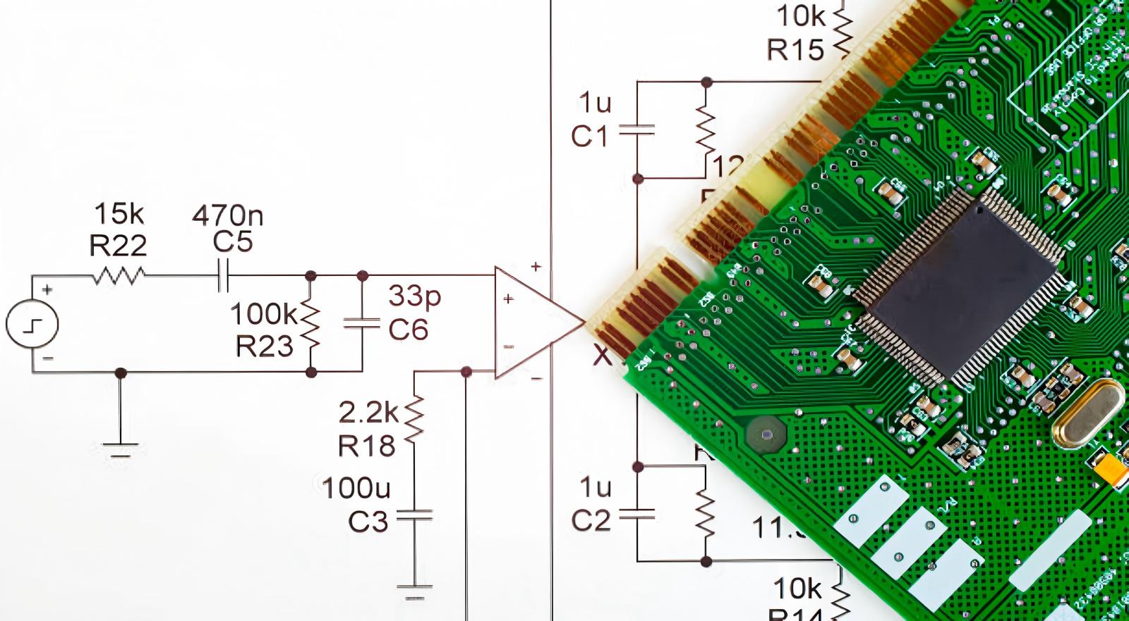
The most successful ESD protection in the design of PCBs is guided by three principles, which include block, divert and isolation. The initial and most obvious way is that the designers need to prevent the entry of ESD into sensitive circuits through the establishment of physical and electrical barriers that prevent the entry of the statical charge into the vulnerable components. Second, they should not allow any incoming ESD currents to pass to ground dangerous through low-impedance paths and have the hostile energy pass through important portions of the circuit. Third, they need to separate sensitive components and circuits with high risk zones where ESD is most probable, e.g., PCB edges, and external connectors. The loop areas, parasitic inductance, discharge paths and consistent, reliable grounding, which are major factors in effective ESD protection, should be minimized in all design choices, including the layer stack-up as well as component placement.
Anti-ESD Techniques in PCB design
Layer Stack-Up: The Basics.
Multi-layers PCBs are superior to the double-sided boards because they decrease the common-mode and inductive coupling to 1/10 to 1/100. Locate signal layers next to a power/ground plane in order to shield the signal, inner layers in high-density PCBs. In the case of double-sided boards, tight power-ground grids (≤60mm, preferably ≤13mm) should be used and openings on power/ground planes should not be more than 8mm. In case openings are required, then continue with narrow traces.
Strategy Layout: ESD Entry
Focus the external connectors on a single side in order to confine ESD entry points. Position sensitive (analog sensors - reset lines) at the center of PCB, not close to edges. Install a minimum 2.5mm perimeter ring ground that has a 0.5mm separation to prevent loops, and is connected through a 13mm via. Keep an isolation distance of 0.64mm between the chassis and the circuit ground and tie them together at 100mm. Fill unoccupied spaces with copper, and ground large fills (≥25mm×6mm) at both ends to avoid the accumulation of static. Leave solder resist off unshielded ground on rings to serve as ESD discharge electrodes.
Routing Best Practices
Signal traces must be kept short, connector traces in particular. Add parallel ground lines to traces longer than 300mm. Use long traces with signal and ground alternating positions; Use long trace routing by using return paths with signals; Minimize areas in loops. Protect parallel route signals (protected and unprotected). Communicate ground lines along signals in ESD prone regions. Filter reset/interrupt lines, move out of edges/ I/O circuits. Center power cords; install bypass capacitors between the power connectors and the IC power pins, at least 80mm distance.
Component Selection & Placement
Install TVS diodes, MLVs, or GDTs within 3mm of connectors with short thick wires (length <5×width) grounded. Install filter capacitors at connector (≤25mm away receiving circuits). Install series resistors/magnetic beads on ESD-prone drivers/receivers without unintentional conductive paths through magnetic beads. Install I/O circuits close to connectors; attach mounting holes to ground (or isolate) with zero-ohm resistors, with large solder-resist-free bottom pads.

Assembly & Chassis Integration
Mount using screws with holes that are equipped with washer (no soldering) so that it makes tight contact with metal chassis. Install PCBs without opening inside the chassis. In the case of multi-board configurations, ESD-sensitive PCBs must be put at the center. Do not apply solder mask to unshielded chassis ground wires to serve as ESD discharge electrodes.
Anti-ESD design effectiveness must be verified through testing PCB designs that are in compliance with the international standards like IEC 61000-4-2 that involves both contact (direct touch) and air (non-contact) discharge tests. Test voltages differ depending on the application: consumer electronics use 4kV -8kV, industrial equipment 8kV -15kV, and automotive and harsh environment uses 20kV and higher. In case a design does not pass these tests, revision should be done, e.g., by reducing the length of ground paths, or adding extra ESD protection devices, refining layout and routing, etc. until the design passes.
Anti-ESD design is not an ad-hoc practice, but a deliberate proactive design that needs to be incorporated in all phases of PCB design, rather than implemented as an afterthought. Through these detailed approaches, designers will be able to develop PCBs that successfully survive in the real-life ESD exposures, and provide quality, stable electronic products. Electronic devices are shrinking, getting more integrated, more sensitive, the focus on the rigor of anti-ESD design is only increasing, and PCBX is determined to continue to be the leader in designing the best ESD protection, making sure that its products are the best in terms of durability and performance.
Hot Tags:

Contact us

If you can't find what you're looking for, please contact us.
Article

Signal reflection in PCBs, due to impedance mismatches, can be managed with impedance matching, termination methods, and strategic layout to ensure reliability.
 2025/09/09
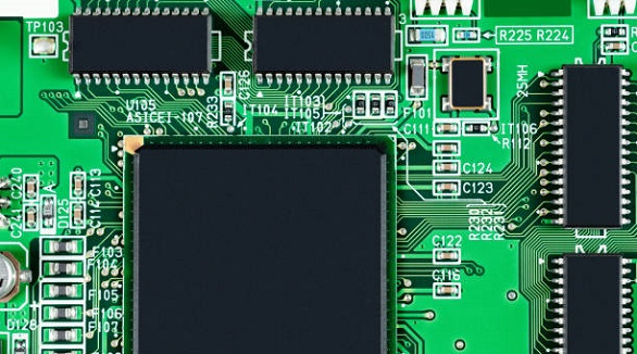
ESD standards like ANSI/ESD S20.20 protect electronics from electrostatic damage, ensuring product reliability and reducing risks in manufacturing.
2025/01/07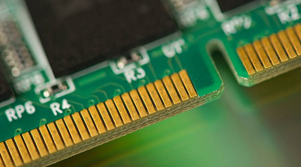
Edge connector bevelling enhances PCB durability and reliable connections, vital for frequent usage and secure engagements, with limitations primarily in plating.
2024/12/25