- Products & Capabilities

- About
- Resources
Best Practices for PTH Soldering


PTH soldering provides strong connections by threading component leads through PCB holes, requiring meticulous preparation and quality checks for lasting results.
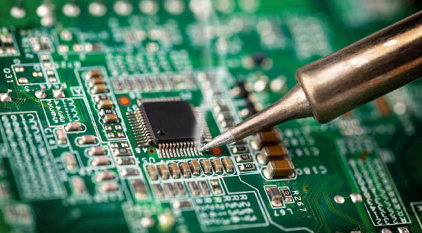
In electronic manufacturing, soldering is an essential skill, especially when installing components on printed circuit boards (PCBs). Of the numerous processes employed, Plated Through-Hole (PTH) soldering, also known as conventional assembly, is an established method. The process involves inserting the leads of components into holes that have already been drilled on the PCB and soldering them to hold them in place. It gives good mechanical and electrical connections, and it is invaluable where component ruggedness is a requirement. This article covers the best practices used in PTH soldering, based on traditional experience and newer developments, to optimize performance and ensure repeatability of results.
PTH soldering differs from surface mount technology (SMT), which connects components directly onto the PCB surface. In PTH, or "pin through hole," components have the leads passed through the PCB holes and soldered, providing good mechanical strength. This characteristic is best applied to applications where there is a requirement for strong interconnections, e.g., in early computers and television manufacturing, where there was minimal space constraint. The solder connections made with PTH are much stronger, appropriate for components that are most likely subjected to mechanical stress.
The Basics of Solder
It is necessary to understand soldering first before entering into the intricacies of PTH soldering. Solder, by traditional definition, is an alloy of lead with large tin content and additions of other metals for special properties. Lead-based solder gives excellent electrical contact and mechanical strength, but environmental effects, particularly lead poisoning, have necessitated alternatives. Consequently, lead-free solders now occupy the market, driven by regulations like the EU RoHS directive in 2006. Lead-free solders, typically tin with copper and silver, provide much the same ability without the health hazards.
Pre-Soldering Preparations
The secret of any successful soldering exercise is meticulous preparation:
Tool Selection: The soldering iron must be fitted with temperature control and an appropriately sized tip to suit the components to be soldered. Rosin-core solder must be utilized due to its controlled flux application, which is paramount to smooth and consistent solder flow.
Surface Cleanliness: All surfaces to be soldered must be clean. Cleaning removes contaminants that may interfere with solder bond quality, such that the metal surfaces are ready for solder adhesion.
Component Fit: Inspect the component lead fit in PCB holes. Good fit minimizes soldering problems and ensures joints created are safe.
The PTH Soldering Process
The actual soldering process entails technique and practice:
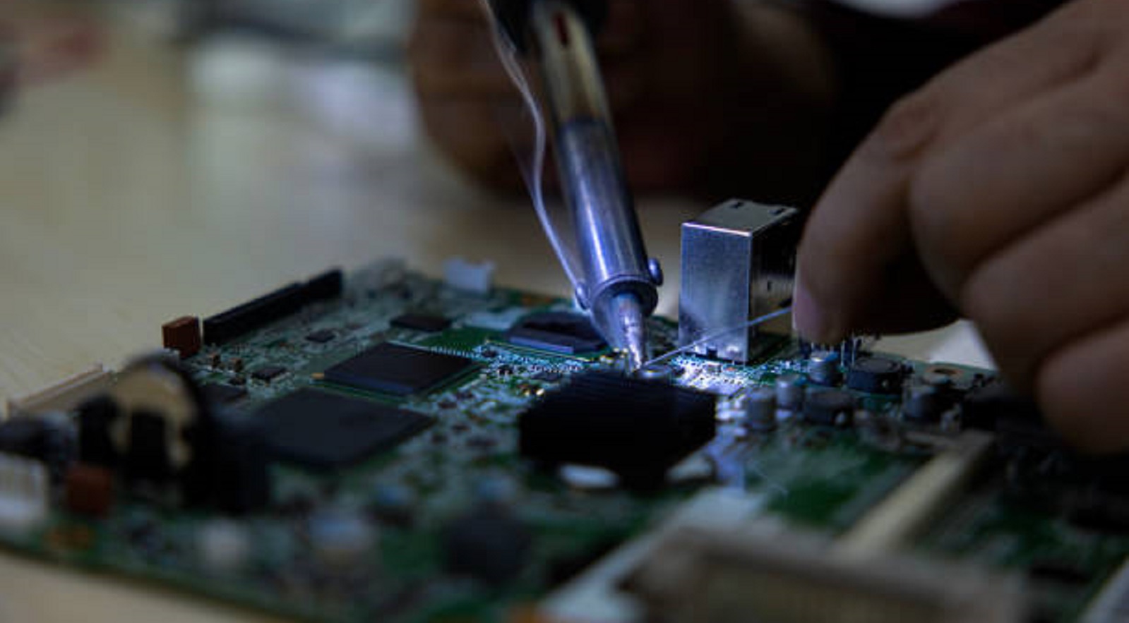
Initial Solder Application: Start by warming a small amount of solder at the tip of the soldering iron. This step assists in transferring heat efficiently to the joint.
Component Placement: Insert the component leads into the holes of the PCB. Hold the tip of the soldering iron on both the lead and the contact pad to supply even heat.
Feeding of the solder: Feed the solder into the joint, allowing it to fill the hole and form a good fillet of solder around the lead. Use enough solder in the hole for a good joint.
Cooling: Remove the soldering iron and let the joint cool undisturbed. The cooling period is crucial so that no disturbance may cause poor joints.
Quality Assurance
For achieving maximum quality in PTH soldering, there must be constant monitoring for consistency:
Visual Inspection: Examine solder joints visually through magnification. Look for surface defects such as voids or incomplete flow.
Electrical Testing: Perform continuity testing with a multimeter to ensure proper electrical connections and function.
Challenges
Even with its advantages, PTH soldering comes with challenges:
Component Fitment: Ensuring correct hole size and annular ring size is important in order to avoid component fitment issues.
Thermal Management: Use thermal reliefs on ground pins to manage heat dissipation to prevent issues like dry or cracked joints due to excessive heat loss.
Design Optimization
PCB design optimization for PTH soldering can simplify the process to a great extent:
Correct Pad Designs: Having the pad and hole sizes as per manufacturer specifications optimizes soldering.
Thermal Relief Patterns: Use thermal relief patterns in the design of the PCB to prevent instant heat loss during soldering. The patterns sustain the heat handling and the joint integrity.
SMD Component Placement: Where possible, place all SMT components on a single side of the PCB. Automating the soldering can be done in this way at the expense of labor but with added efficiency.
Tools for PTH Soldering
Having the proper tools will enable one to carry out PTH soldering effectively:
Soldering Irons: Choose soldering irons with temperature control for added precision and better heat management.
Solder Vacuum: Also known as solder sucker, the device is used to remove excess solder easily in desoldering, helping in corrections or repairs.
Solder Wick: Useful in solder removal from joints and soldering error correction. It is an eraser in your soldering tool set.
Flux Pens: Uses flux application over tricky areas to facilitate flow of solder, enhancing overall look of a joint.
To excel at PTH soldering, you must know, practice, and adhere to best practices. With care in preparation, correct tool handling, delicate techniques, and rigorous quality checks, electronics manufacturers can achieve consistent and durable connections. As technology keeps evolving, adherence to these best practices ensures continued excellence in PCB assembly. Should you require further assistance or personalized guidance, the experts at PCBX can help you overcome any challenges you may encounter. When properly implemented, PTH soldering can be a strong and stable process in your electronic production venture.
Hot Tags:

Contact us

If you can't find what you're looking for, please contact us.
Article
Solder masks protect PCBs from damage and solder bridging. Available in various types and colors, they ensure reliability. Eco-friendly options and precise thickness measurements are crucial for quality.
 2024/10/08
Wave soldering is vital for assembling printed circuit boards (PCBs), aiming to bond electrical components. The process involves passing PCBs over a wave of molten solder to form connections. Common defects include pin/blow holes, solder shorts, poor hole fill, lifted components, excessive solder, solder balling, and solder flags. To address these issues, key factors include proper flux application, controlled preheat temperatures, optimal solder wave settings, and careful material handling. Understanding and managing these factors ensures high-quality, reliable PCB assemblies.
2024/09/05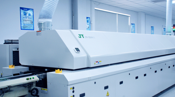
Soldering forms a very important part in the assembly of a PCB. Wave soldering is ideally applied in Through-Hole Technology, while reflow soldering in Surface Mount Technology. Wave soldering involves flux spraying, pre-heating, soldering, and cooling, while in the case of reflow soldering, pre-heating, thermal soak, soldering, and cooling steps are applied. Temperature and time control are the two most critical parameters in the above-mentioned techniques for ensuring soldering reliability.
2024/07/26