- Products & Capabilities

- About
- Resources
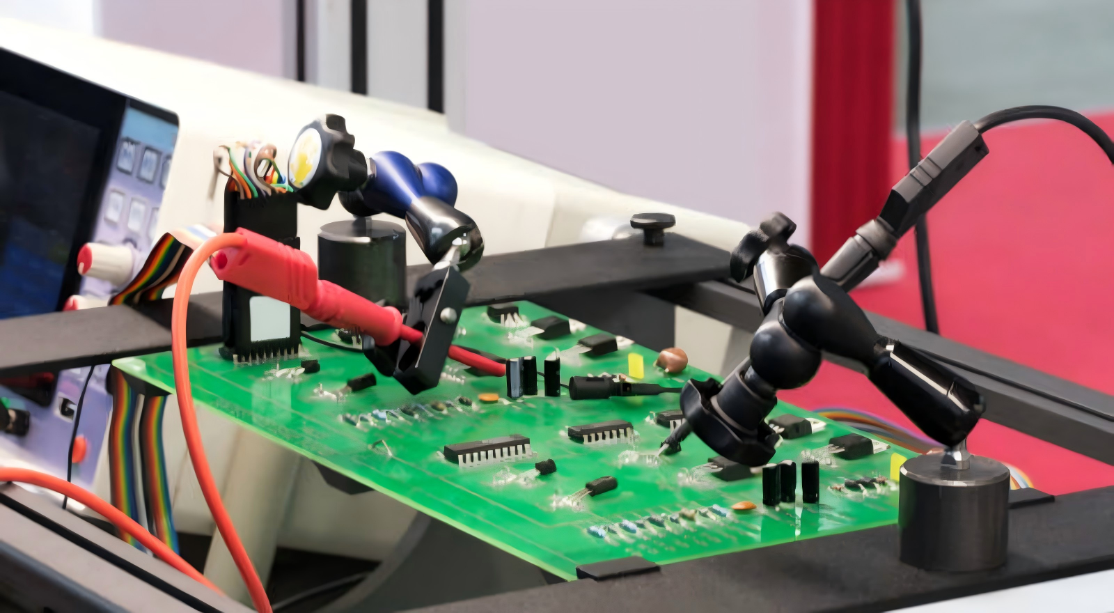
Design Mistakes that Lead to PCB Assembly Errors


Learn common PCB design mistakes that cause assembly errors and follow DFM best practices to improve PCBA yield and reliability.
With the development of modern electronic manufacturing process, printed circuit board assembly (PCBA) quality is largely determined by PCB design at the early stage of the production. There are some common assembly problems like tilting, solder bridging, inadequate soldering, and poor paste printing, which may not be the direct fault of the production process, but can be attributed to the unreasonable schematic and layout design of the initial stage. Failure to consider manufacturability in design will significantly add to the complexity of the assembly process, increase defect rates, lengthen production cycles and add rework costs. The most prevalent PCB design problems and their associated assembly issues are addressed and discussed in this article, along with some useful tips for optimizing the design.
Unreasonable Pad Design
The three basic factors that determine the quality of soldering are size, shape and spacing of the pads. The common error is to make pads that are too small to mount on the surface. A narrow pad will allow minimal solder paste to be printed and is susceptible to cold solder joints, component falling off and weak soldering points after reflow soldering.
By contrast, oversized pads result in too much solder being deposited and solder bridging between neighboring pins and short circuits. Illegible looking pads and an unequal layout of pads on dual-ended parts are also frequent design flaws. This layout is sure to cause non-uniform solder tension on melting, and give the classic solder tombstoning phenomenon which is an upward lift of one end of chip resistors and capacitors.
Also, it is difficult to get the solders to penetrate the layers if the pad openings are not consistent in both top and bottom layers, particularly for through-hole component assembly and for making stable connections. The standard pad size should be determined strictly according to the component datasheet and SMT production capability by the designers.
Improper Trace Routing Arrangement
Multiple hidden troubles on PCB assembly arise from disordered trace routing. Firstly, the thin traces and ultra narrow trace spacing make the etching process more cumbersome for production, as well as solder leakage and short circuit in high-density assembly. Excessive parallel traces will also cause signal interference and have an impact on subsequent manual welding and maintenance.
Secondly, it will eliminate uniform heat conduction during reflow soldering when the routing is routed directly next to the edges of components and/or in the thermal balance area. If there is poor heat distribution or over heating around the components, the solder may not melt uniformly which further adds to soldering problems. Large area copper pours are another area that many designers fail to consider thermal relief routing. Massive heat accumulates slowly over complete solid copper surfaces to dissipate which results in extended heating times, component heating and soldering batch variations.
Furthermore, around connectors and plug-in locations, concentrated dense routing will hinder workers' and automated equipment's smooth plug-in, welding and testing operations, leading to operating space issues during the assembly process.
Failure to FollowComponent Layout Rules
Unstandardized component layout is one of the main sources of assembly errors. If heavy large size parts are placed on one side of the PCB without weight balance design, it will bend and warp during the high temperature soldering process, and cause loose soldering and displacement of the components.
Another problem is combining tiny fine pitch chips or chips with very high volume power devices in a small space. There are significantly different peak reflow soldering temperature characteristics for different components. When the concentrated layout is adopted, it is difficult to satisfy the welding temperature requirement of all the components simultaneously due to unbalanced local temperature field.
The batch reverse mounting errors are easily caused by placing polarized parts like diodes, electrolytic capacitors and integrated circuits in an unreasonable direction when assembling the product in mass production. In the meantime, attaching sensitive precision parts to near heat-producing power modules will not only impact electrical performance, but also shorten component aging time and raise the failure rates after assembly. Also it is often forgotten that it is necessary to have the assembly clearance reserved, which is necessary for proper placement of the components by placement machines and makes it harder to carry out the glue dispensing and cleaning operations in subsequent stages.
Deficient Manufacturability Considerations
Numerous design schemes are only concerned about electrical performance and disregard the principles of DFM (Design for Manufacturability). Excessive hole depth and small hole diameter cause blind vias and buried vias to be hard to process in traditional assembly plants, which results in problems with hole filling, tin plating, or open circuits.
The board outline design is unreasonable and has sharp corners and irregular notches and missing positioning fiducial marks, which will cause positioning deviation in the automatic placement, resulting in overall positioning deviation when assembling the components by the solder paste printing machine. Also, designers rarely leave adequate test points and process edges. Due to the absence of test points, the defective circuits can only be discovered after assembly, which takes a lot of time; insufficient process edges can not satisfy the clamping and transmission requirements of the assembly equipment.
There are no unified design rules for multi-layer PCB design. It is an inconsistency of the alignment deviation of the layers which will lead to disorder of the circuit connections inside the layers, which will become apparent only after assembly and will ultimately manifest as the failure of the circuit.
Inappropriate Thermal Management Design
The use of unreasonable thermal layout design will lead to various continuous assembly and use failures. Multiple high power heating elements are concentrated on layout, resulting in overheating at local spots on PCB. High temperature will not only alter the physical properties of the solder joints resulting in desoldering, but also deform the substrate and part the layered boards.
If there is no independent heat dissipation copper area and heat dissipation via for heat dissipating components, the heat can not be exported timely. During the reflow soldering process, the local overheating will cause the plastic shell of the components to burn and make the internal core components burn. A single cooling speed design causes the internal stress to be produced in the circuit board, which leads to the occurrence of hidden crack defects in subsequent use, and also causes the cooling speed to be uneven after welding.
When it comes to PCB assembly errors, most of them can be avoided if there are some errors made in the early design stages. The qualified PCB design should start from the premise of electrical performance, and comprehensively integrate SMT assembly technology, production equipment parameters, component characteristics and DFM manufacturability standards. To reduce assembly defects, pad optimization specifications, standardizing trace routing, scientific component layout, perfecting pad auxiliary process design, and improving the thermal balance layout are all crucial steps.
The designer must draw up the design concept and make a full process design review before formal production on the board, and communicate with the PCBA manufacturers in time to modify the unreasonable details. The only way to significantly reduce the rate of assembly defects, thereby maintaining product quality throughout manufacture, shorten the manufacturing cycle and effectively control the total cost of electronic products production is to overcome design problems with hidden dangers at the beginning.
Hot Tags:

Contact us

If you can't find what you're looking for, please contact us.
Article

Controlled impedance is crucial in modern PCBs, ensuring signal integrity through precise trace and material design, essential for high-speed applications.
 2025/01/24
Power and ground planes in PCBs ensure signal integrity, manage heat, and minimize EMI, crucial for efficient, high-performance electronic devices.
2024/11/11
DFM ensures cost-effective PCB design by optimizing size, layers, materials, and components, focusing on manufacturability, reliability, and process efficiency.
2024/10/30