
- Products & Capabilities

- About
- Resources
Design Tips for Stable Crystal Oscillators on High-Density PCBs


Gain practical tips to optimize crystal oscillator stability and avoid frequency drift in high-density PCB designs.
A crystal oscillator is the basic timing heartbeat for today's electronic systems. They can create very stable resonant frequencies by the piezoelectric effect of quartz crystals, which can then be used for reliable synchronization of microcontrollers, processors, communication interfaces, and RF circuits. With the advancement of electronic products miniaturization, high integration and multi-function, high-density PCB design has become the mainstream of portable products, industrial control and high-speed communication products. But, the small size, high routing density and mixed signal environment of high-density PCBs are challenging the crystal oscillator stability. Often frequency deviation, increased phase noise, signal jitter, and system start-up failure occur due to parasitic capacitance and inductance, electromagnetic interference (EMI), thermal drift, and insufficient grounding. The article examines the major design issues associated with crystal oscillators in high-density designs on printed circuit boards and offers a variety of practical, engineering-tested techniques for layout, grounding, EMI rejection and impedance matching. To make sure engineers get consistent, reliable timing performance at any time, anywhere on the board, these rules can be followed.
Key Challenges to Crystal Oscillator Stability in High-Density PCBs
The density of the PCB design restricts the placement of components and routing of traces, thus presenting special risks to crystal oscillator operation.
The first problem is the parasitic capacitance and inductance. The components are tightly packed, trace lengths are short and vias are dense, adding unwanted stray parameters to the oscillation loop. The parasitics alter the overall load capacitance and resonance, affecting the output frequency of the crystal and making it less stable when oscillating.
Second, sensitive timing circuits are very susceptible to electromagnetic interference. Strong high frequency noise is produced by high speed digital traces, switching power supplies and RF modules. With compact designs, this noise can couple to crystal traces through capacitive or inductive paths, leading to jitter and unstable oscillation.
Thirdly, thermal effects affect the accuracy of frequencies. The hot spots and temperature gradients are generated by concentrated heat from the power components. Quartz crystal frequency is very sensitive to temperature and thermal drift is the principal source of long-term instability.
Finally, the internal structure of the crystal is altered by mechanical stresses due to bending, assembling and vibration of the PCB, which result in short-term frequency changes, called microphonic effects. The combination of these factors makes the optimization of stability important in high density designs.
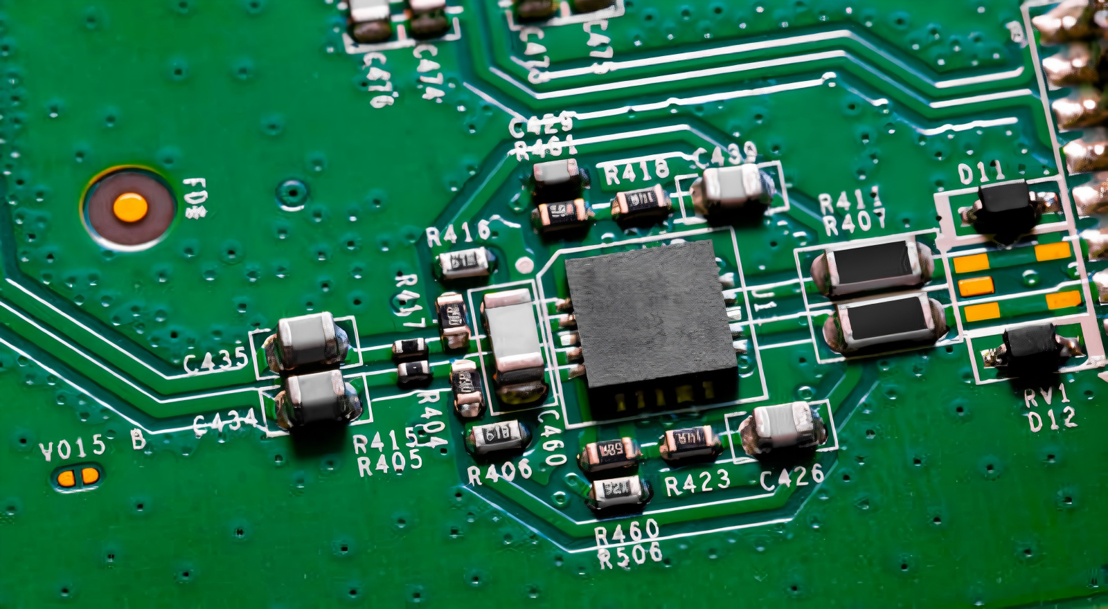
Layout Best Practices for Stable Crystal Oscillator Performance
Reliable operation of a crystal oscillator will only be achieved with careful physical layout. There are a number of rules that must be observed to reduce parasitics and interference.
Firstly locate the crystal and load capacitors very near to the IC oscillator pins. The parasitic capacitance and inductance is minimized by maintaining trace lengths below 10 mm, and this directly contributes to frequency stability.
Second, for a crystal and load capacitors use short, straight, symmetrical traces. As far as possible avoid trace loops as these function as antennas and pick up unwanted EMI. Symmetric routing balances the oscillator loop, and gives better noise immunity.
Thirdly, separate the crystal circuit from fast speed and high power devices. Rotate away all the regulators, clock drivers, and RF circuits from the oscillator space. Use guard rings or physical barriers for limited isolation to minimize coupling. If traces need to cross, make sure they cross at right angles to reduce the crosstalk.
Stable Grounding Techniques for Greater Stability
The stability of crystal oscillators is important in the ground design. Loss of grounding produces noise paths and distorts the signal.
The dedicated ground plane under the crystal circuit creates a low impedance return path and helps to minimize EMI. Do not divide the ground plane under the oscillator as gaps add loop inductance and noise.
Ground vias need to be located directly at the load capacitor pads to connect to the ground plane in a short, low-inductance path. This practice eliminates ground bounce and maintains clean signal reference.
For mixed-signal systems, use two different grounds; connect them together around the power supply. This keeps the switching noise from the digital switching circuit from fouling the delicate analog oscillator circuit. An earthy guard ring around the crystal also eliminates lateral electromagnetic coupling.
EMI Reduction and Impedance Matching Strategies
In a high density and noisy environment the suppression of EMI and impedance matching are critical for accurate frequencies.
Add 0.1 μF to 1 μF bypass capacitors at the power input to reduce the high frequency ripple, to filter EMI. The metal shields are fully grounded when there is a harsh environment, they can effectively block external interference. The series resistors also help to control signal rise times, which reduces EMI emissions.
Impedance matching is a way to guarantee that the oscillator runs at a set frequency. The total capacitance of the PCB plus the load capacitance of the crystal (usually 12-20 pF) must be the same. One of the most frequent reasons for frequency shift and unstable start up is mismatched load capacitance. On high frequencies (30MHz and above) controlled-impedance traces prevent signal reflections and preserve the integrity of the signal shape.
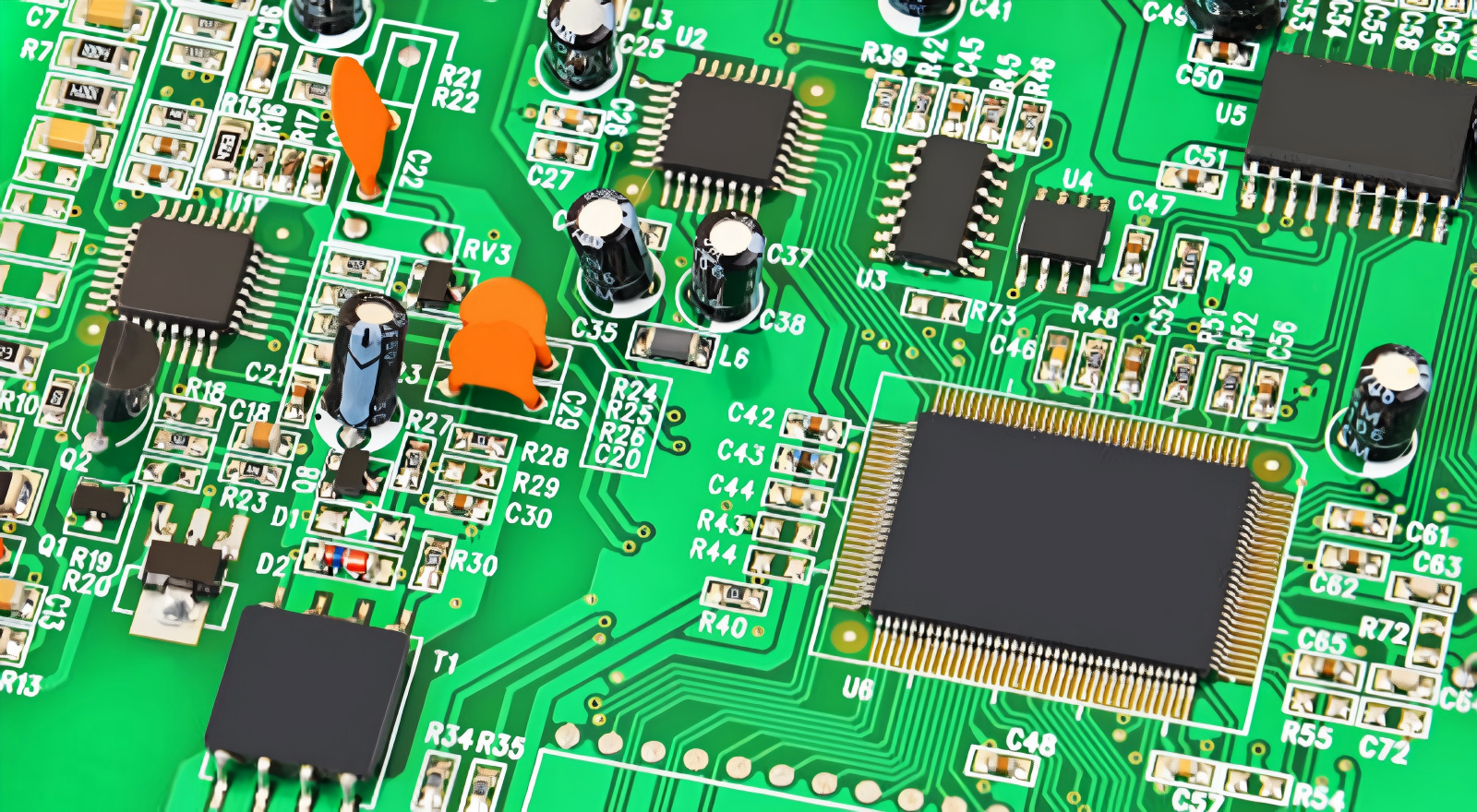
Additional Recommendations for Long-Term Stability
In addition to layout and routing, the selection and verification of components is vital. For high precision applications select crystals with a low tolerance(±10 ppm or better). TCXO (Temperature-Compensated Crystal Oscillators) are ideal for wide temperature applications with stability of ±0.5 ppm from -40°C to 85°C.
Pre-production parasitics and noise is determined using design simulation and real-environment testing. Minimized mechanical stress and contamination from strict assembly practices, like controlled soldering temperature and cleaning, mean better performance over time.
Designing for max stability of crystal oscillators in high-density PCB designs requires a step-by-step design methodology, which includes careful layout, strong grounding, good EMI rejection, and proper impedance matching. Engineers can design reliable timing circuits even with a very compact design by mitigating parasitic effects, thermal drift and mechanical stresses. These practices guarantee a consistent operation across consumer, industrial and communication applications, with low jitter and minimum frequency drift.
PCBX offers industry-leading expertise in timing circuit design and high-performance PCB development. With advanced engineering support and a focus on stability and reliability, PCBX helps designers transform complex high-density layouts into robust, production-ready electronic systems.
Hot Tags:

Contact us

If you can't find what you're looking for, please contact us.
Article
PCB tolerances ensure PCB reliability and performance by managing allowable variations in dimensions and materials, crucial for manufacturability and quality.
 2025/04/08
eFuses are advanced PCB fuses that reset automatically, offering fast, precise protection and versatility in electronics, enhancing device safety and reliability.
2024/11/12
Thermal management is all about more than just keeping the temperature of electronic systems and printed circuit boards low. It has been a key issue related to reliability and performance. Of the very basic fundamentals that would be studied in the field, some are concerned with methods of heat transfer. These are through conduction, convection, and radiation. The methods of cooling include natural cooling, forced-air cooling, fluid cooling, and evaporation cooling. Appropriate thermal design rules shall be followed wherein the chosen materials provide optimum thermal conductivity and the components of a system are so laid out that no hot-spotting will take place. Thermal analysis becomes critical in pointing out heat-related issues and optimizing the design. It thus minimizes failure rates and enhances stability and functionality of the electronic systems through comprehensive thermal management.
2024/07/25