- Products & Capabilities

- About
- Resources
Essential Guide to PCB Potting & Encapsulation


Learn professional circuit potting steps for reliable electronic encapsulation to protect PCBs from vibration, moisture, and harsh industrial environments easily.
Electronic circuits are frequently exposed to moisture, dust, chemical attack, severe vibration, thermal shock and cycling. Unprotected, delicate components and solder joints can fail from wear, shorting, and even complete breakdown. Potting, or full encapsulation, is the best way to protect printed circuit boards from harsh environments by encapsulating them in a protective coating of liquid insulating resin that solidifies to form a solid shell.
The Benefits of Potting and Encapsulation
Potting differs from thin conformal coating that merely coats components and wires, by completely encasing all elements, wires and solder joints within a solid or flexible resin shell. This complete coverage offers several benefits. It offers excellent environmental protection against moisture and chemicals, enhances mechanical robustness against vibration and shock, increases electrical insulation to avoid leakage and short-circuiting, facilitates better heat dissipation for thermal management, and even helps to prevent tampering for security of circuit designs. For automotive components, industrial control units, outdoor sensors, and medical equipment, well-potted products enhance both reliability and lifespan.
Three Main Types of Potting Compounds
The quality of potting compound defines the quality of the potting. Epoxy resin has good mechanical properties, superior chemical resistance and minimal shrinkage, making it suitable for indoor industrial applications and high-rigidity products. Silicone materials have superior flexibility and extreme temperature range from -50°C to 200°C for excellent thermal cycle fatigue resistance, which are suitable for outdoor exposure and high temperature applications. Polyurethane exhibits average flexibility, impact strength and rapid cure speeds, making it ideal for mass production of consumer products and general low-power circuit boards.
Step-by-Step Potting and Encapsulation Operation
Prepare Workspace, Tools and Materials
First, set up a clean, dry and well-ventilated workspace. Maintain a temperature of 20°C-25°C in the room to maintain the resin's viscosity and curing performance. Gather the electronic PCB assembly, potting compound, plastic or metal housing, measuring instruments, clean mixing containers, mixing sticks, vacuum degassing device and safety protection gear including gloves and safety googles. Ensure that the working environment is clean from dust, hair, and other contaminants that may lead to weak adhesion and internal voids in the cured product.
Clean, Prepare and Mask the Circuit Board
Thoroughly check the circuit board for damaged components, broken leads, cold solder joints and damage. Fix any problems before potting, as they will be impossible to repair once potted. Carefully clean the PCB surface with isopropyl alcohol and lint-free cloth to remove flux, oil, and dust. Let the board dry for some time. Finally, protect all external connections, charging ports, sensor test points and test points that need to be accessible with high-temperature masking tape.
Accurately Mix the Potting Compound
High-performance potting compounds are usually two-component materials (resin and hardener). Always use the officially recommended weight ratio. Before mixing, add the two parts into a dry container and mix gently for three to five minutes. Make sure to scrape the bottom and walls of the container to prevent unmixed areas. Do not stir fast because this will incorporate a large number of bubbles. Once mixed, pour liquid resin into a vacuum chamber for a few minutes to eliminate micro bubbles to avoid encapsulation voids.
Slowly Pour Resin into the Enclosure
Slowly position the washed PCB in the center of the enclosure to ensure that resin covers all sides. Slowly pour the resin mixture from one side of the enclosure, allowing it to flow across the board and over all components. Do this in multiple batches if the circuit has dense components with high standing capacitors and small chips. Once filled to the standard fill line, leave some space at the top for expansion. Tap the enclosure on the desk to get rid of the last few small bubbles.
Controlled Curing and Post-Inspection
The curing process determines the final hardness and protection. You can select room temperature curing (24 to 48 hours) or low-temperature heating curing (60°C to 80°C) to reduce the curing time. Make sure the enclosure is free from vibration during curing to prevent layer unevenness and stress. Once cured, carefully remove the masking tape, cut off extra resin, and check the surface for any cracks, bubbles or unfilled areas. Lastly, test the circuit's full functionality by turning on the electricity.
Tips on How to Prevent Potting Defects
For the best encapsulation, avoid over-filling the resin, keep the environmental temperature strictly and don't be too anxious about the curing process. Bubbles, delamination and cracking are the most common potting defects, usually due to insufficient cleaning, too fast stirring, improper mixing ratios, and fluctuating curing conditions. Selecting a resin with a similar thermal expansion coefficient as the PCB material can also minimise component stress due to temperature fluctuations.
Understanding circuit potting and encapsulation is key to electronics manufacturing. By choosing the right material, proper preparation and rigorous operation step-by-step, you can significantly enhance circuit reliability and product lifetime. For quality PCBs, assembly services, and encapsulation, PCBX offers comprehensive electronic manufacturing services to ensure the best performance and reliability for your projects.
Hot Tags:

Contact us

If you can't find what you're looking for, please contact us.
Article
PCB encapsulation offers vital protection against environmental, mechanical, and security threats, ensuring the reliability and longevity of modern electronic devices.
 2025/01/17
PCB standoffs secure PCBs by spacing them, aiding in thermal management and vibration absorption. They're key for durability and adaptability in electronics.
2024/12/09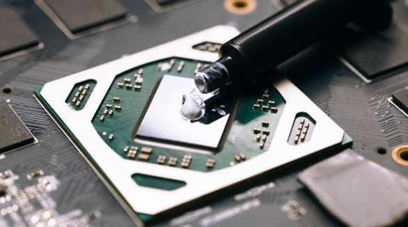
PCB glue secures and insulates components on PCBs, enhancing stability and durability under various conditions in electronics from consumer to aerospace uses.
2024/11/25