- Products & Capabilities

- About
- Resources
Essential Tools and Techniques for PCB Assembly


PCB assembly requires soldering, proper manual/automated tools, key techniques and best practices to ensure quality.
PCB assembly requires soldering, and does not depend on whether you are a beginner or not. It is an art that creates the difference between a good and a bad circuit board; one that has weak connections or short circuits. PCB assembly is the link between the electronic design and the functional device that the quality of the assembly directly depends on how reliable and long-lasting a product will be.
Essential Tools for PCB Assembly
The choice of your tool is based on the size and the complexity of your PCB assembly project. The breakdown of both manual and automated workflow tools is as detailed below:
Tools for Manual Assembly
Small-batch prototyping and hobby projects may use manual tools, focusing on accuracy and convenience:
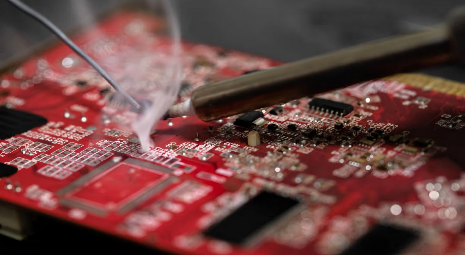
Soldering Iron: A variable power (25-60W) soldering iron with a fine tip (0.5-1mm) is necessary when working with small surface-mount devices (SMDs). Microcontrollers are delicate and demand temperatures around 260℃, whereas bigger connectors demand up to 350℃.
Solder Wire: Solder of choice is Rosin-core solder (0.5-1mm diameter). Beginners can use led solder (melting point 183℃) and lead-free alternatives (melting point 217℃) are environmental friendly and meet safety standards.
Desoldering Tools: A desoldering pump (applies a vacuum force) or desoldering wick (absorbs excess solder) corrects errors without harming the PCB.
Supporting Equipment: Anti-static tweezers (to work with small parts), a magnifying glass (to see tiny joints), a flux pen (enhances the solder flow), and an anti-static wristband/mat (guarantees components are not discharged during electrostatic operations, ESD).
Tools for Automated Mass Production
Speed, consistency and precision in large-scale production: Automated equipment ensures all three.
Solder Paste Printer: Latent solder paste with laser-cut stencils of 0.1-0.15mm accuracy uniformly on PCB pads.
Pick-and-Place Machine: With SMD place error of 0.05mm and the smallest components, vacuum nozzles and vision systems position SMDs.
Reflow Oven: The controlled temperature curve (150 preheat, 220-250 solder melt, gradual cool) is used to create strong, dependable solder joints.
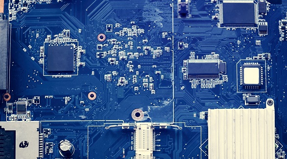
Inspection & Soldering Equipment: Automated Optical Inspection (AOI) systems identify defects; X-ray detectors examine hidden joints (e.g., BGAs, QFNs); wave soldering machines receive through-hole components (THTs).
Major Methods of Successful PCB Assembly
It is paramount to master the basic techniques in order to prevent defects and provide dependable PCB functionality. The following are stepwise procedures of every important step:
Pre-Assembly Preparation
Have this rightly prepared, and you may assemble without mistake:
Check the Bill of Materials (BOM) and make sure that all components per match design characteristics (part numbers, package types, polarities).
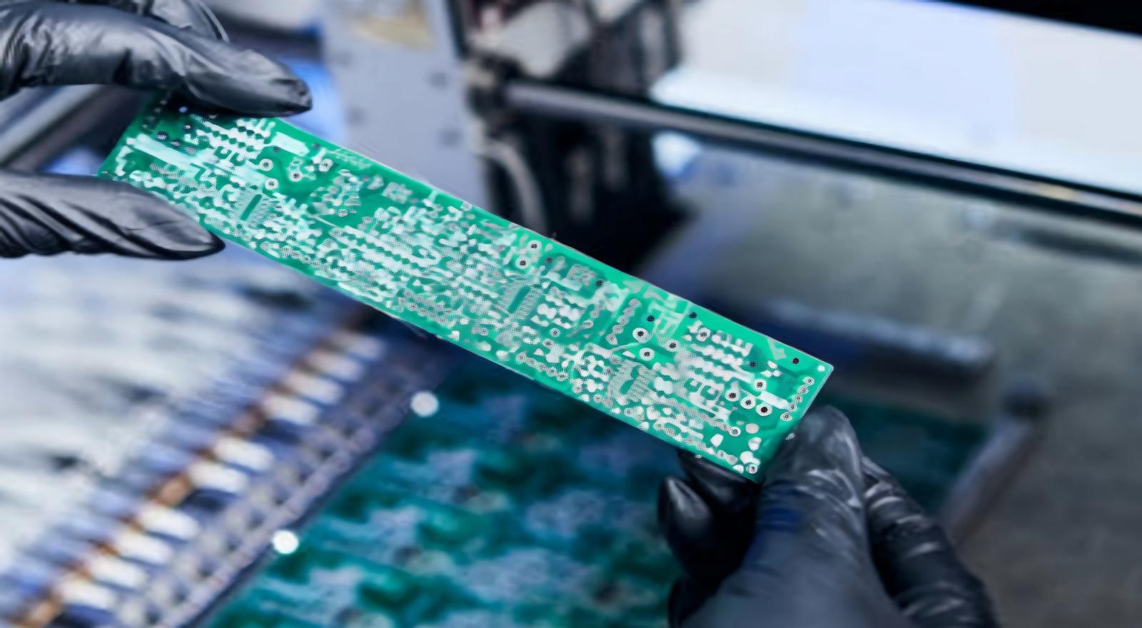
Check the bare PCB scratch, deformation, or bad pads; clean with isopropyl alcohol to clean up.
Keep humidity-sensitive parts (e.g., ICs) in a dry cabinet; store refrigerated solder paste at room temperature (4 hours) before use.
Prepare a well-ventilated, well-lit area and put on safety glasses to save against solder splashes.
Essential Soldering (Introduction)
Take these steps to get clean and reliable solder joints:
Tin the Iron Tip: Coat the tip with a small amount of solder to stop oxidation and enhance heat transfer; wipe off excess solder with a wet sponges or brass cleaner.
Apply Heat & Solder: Heat both component lead and PCB pad together 2-3 seconds; solder the joint (not the tip of the iron) until it forms a shiny, concave joint.
Cool & Inspect: Allow joint to cool naturally (5 seconds); with a magnifying glass inspects dull, grainy cold joints (rework necessary).
Avoiding & Repairing Solder Bridges
Solder bridges (the strands of solder that have spilled over) are the most frequent problem--here's how to deal with them:
Prevention: Use minimum solder, place solder on a 45deg angle and keep the iron tip clean to prevent dragging solder on nearby pads.
Fixing: Over the bridge, place desoldering wick, heat with the iron, and allow the wick to absorb excess solder, then clean the area with isopropyl alcohol.
Component Placement & Rework
Positioning: SMDs should be directly seated on pads; THTs should be seated in through-holes; polar components (diodes, ICs) should be aligned to PCB silk-screen markings (inversion leads to failure). Pick-and-place machines operated automatically require periodic feeder calibration.
Rework: Start with a rework station; desolder THTs with a pump, and SMTs with 300℃ hot air; clean pads with desoldering wick and alcohol and then replace components.
Common Mistakes
Components Overheating: Do not exceed 3-5 seconds of iron contact per joint to prevent overheating.
Excess Solder: Bridges and smothers good connections; apply enough to create a small, even solder joint.
Ignoring Flux: Flux removes surface contaminants and enhances solder flow--never leave out rosin-core solder or excess flux.
Omission of Safety: There must be ventilation and protection during the soldering process.
Best Practices
Keep Tools: Wipe and tin the iron tip after use, filter rework station, store materials in cool dry environment.
Meet Standards: Compliant with ROHs regulations (lead content≦0.1%); assure that tools are used and that they are calibrated; record the assembly process to allow retrace.
ESD Protection: Provide ESD-safe condition (23±5, 30-60% RH) to safeguard delicate components.
Post-Assembly Inspection & Testing
The PCB is inspected and tested to make sure it functions as intended:
AOI/X-ray or visual inspection (assisted by a microscope) to identify bridges, cold joints or misaligned components in mass production.
In-Circuit Testing (ICT) to check continuity of circuits and component values.
Functional Circuit Testing (FCT) to emulate real-world operation and ensure that it works.
Re-work defective parts with a hot air gun and desoldering tools.
PCB assembly is a combination of appropriate tool choice and careful technique. With a little preparation in pre-assembly, basic soldering, defect prevention, and maintaining your equipment, you will be able to make a high-performance PCB that is reliable. You can become an expert in transferring electronic designs into practice, both in a hobby and in an industrial context.
Hot Tags:

Contact us

If you can't find what you're looking for, please contact us.
Article
Functional testing verifies PCB functionality in simulated environments, enhancing quality and reliability, detecting faults, ensuring performance, and cost efficiency.
 2024/10/25
FAI ensures the first PCBA production runs meet design specifications. Automation improves FAI by enhancing efficiency, accuracy, and reducing errors, transforming quality assurance in PCB assembly.
2024/10/09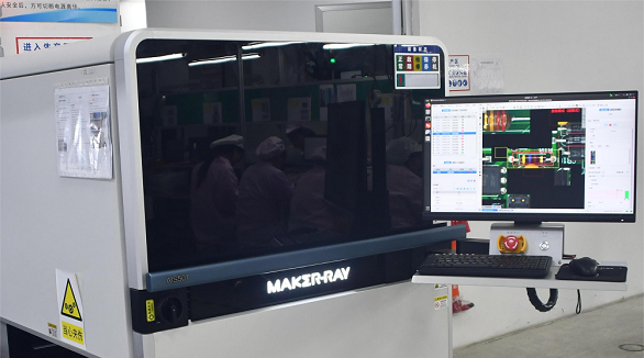
These SMT PCB assembly methods are involved, ensuring that several defects are detected. This includes the use of Automated Optical Inspection, In-Circuit Testing, and Automated X-ray Inspection. The combination of these methods is beneficial in facilitating an optimal inspection process.
2024/07/26