
- Products & Capabilities

- About
- Resources
How to Avoid Pitfalls in PCB Design


Avoid costly PCB design mistakes in footprints, spacing, thermal management, and DFM before production.
A printed circuit board can successfully pass all simulations and yet fail on the assembly line. Most costly PCB design errors occur here: where the design and the actual production vary. When creating a design, the first time you design it properly is when you think about how the board will be built, tested, and used in the field.
Component Footprint and Land Pattern Errors
The common mistake and costs associated with this is when the schematic symbol is not consistent with the actual footprint on the board. If the size of the land pattern is too small or too large for the package size, then it can lead to solder bridging or under-wetting during reflow. This is especially a challenge on a fine pitched component such as a QFN or BGA, where the geometry of the pads has very little tolerance. Designers are cautioned to check footprints against manufacturer's datasheets, not against generic library parts, and be sure to check the correct pad size based on the thickness of the solder paste stencil used in the manufacturing process.
Inadequate Component Spacing and Clearance
When the designer is under pressure to reduce the size of the board, components may be closer together than the assembly process can keep them. Taller components may cause shadowing effects during reflow, where the hot air or infrared is being applied to the shorter components and is being blocked from the taller components by the lack of clearance. The close spacing of fine-pitch ICs and other components also allows little room for placement accuracy, which may result in soldering bridges or tombstoning. As a general principle, the clearance should be based on the assembly process being employed, and the deviation from the clearance should be reported as early as possible, not at first article inspection.

Thermal Management Left as an Afterthought
Thermal design is usually considered a post-layout problem instead of beginning design where thermal design can be a constraint. Components may fail prematurely in the field if proper copper pour, thermal vias, or separation from heat-sensitive components are not included. This point is particularly important for power-dense applications like motor drives or power converters, because heat on or close to switching elements can damage capacitors, ICs, etc., in the future. More often than not, it is easier to consider the thermal aspects at layout phase than to add a heatsink at a later stage.
Signal Integrity Planning at High speed
As the clock rates and data rates continue to rise, cosmetic decisions for trace routes become electrically significant. Unmatched trace lengths on differential pairs, routing high-speed signals over split ground planes or placement of vias inappropriately along a critical signal path can cause reflections, crosstalk or timing skew. These problems are frequently not discovered until a board is really loaded and operating, and thus difficult to correlate to some layout decision, and costly to backtrack to. Fixing routing and return-path continuity issues after a layout has been completed requires a lot of engineering time and is a source of headaches during certain classes.Routing and return-path continuity issues can be a headache time sink that can take weeks of engineering time if not planned for upfront.
Panelization and Fiducial Oversights
Late decision of panelization can lead to additional conflicts at the assembly line. A board without proper fiducial markers, or if the spacing between the individual units on a board is inconsistent, will require manual adjustments which will slow throughput and introduce placement variability. Panelization strategy and assembly line planning should not be done as a formality after tooling has been ordered, but rather should be coordinated when the assembly line is first designed.
Silkscreen and Test Point Neglect
As you approach tape-out, it's easy to forget about the silkscreen legends and test point placement, but they come back to bite you in the rear down the road. Unspecified or incorrect polarity marks on parts such as electrolytic capacitors and diodes can increase chances of incorrect component polarity. Boards with inaccessible test points are also slower and less predictable when it comes to in-circuit testing and functional debugging, especially during the initial production volumes, where every second counts to get the product to market.
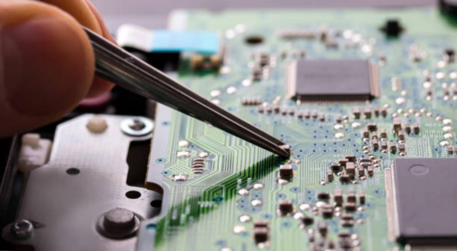
Overlooking Manufacturer-Specific Design Rules
The generic design rule checks (DRC) in the EDA tools are useful for detecting obvious problems (e.g., width of traces, unconnected nets, etc.) but don't consider the specific usability and tolerances of the fabricator that is going to build the board. The minimum trace and space requirements (aspect ratios), as well as copper weight limits, differ from one manufacturing house to another and a design that passed through a generic DRC could still need expensive rework on one particular production line. This gap is closed when the design files are shared with the fabricator before finalizing the design layout, rather than after it is finalized.
What is common to all of these pitfalls is that manufacturability and reliability issues are much easier to overcome in the design phase than once fabrication or assembly starts. Placing a habit in the early and repeated review of footprints, thermal risks, signal integrity problems, and DFM conflicts before Gerbers are sent out, tends to result in boards that pass first article inspection without a lot of surprises and get to volume faster.
Hot Tags:

Contact us

If you can't find what you're looking for, please contact us.
Article
PCB failures due to minor orientation and polarity errors can impact reliability, but proper design practices and checks ensure manufacturability and performance.
 2025/12/18
Castellated pads in PCB design facilitate easy board-to-board connections, enhancing miniaturization, assembly, solder quality, and flexibility for compact modules.
2025/01/13
Capacitors are crucial in PCB design for filtering and timing. Correct polarity in electrolytic and tantalum types prevents malfunctions and ensures reliability.
2025/01/09