- Products & Capabilities

- About
- Resources
How to Do ESD Protection During SMT Assembly Process?


Effective ESD control in SMT assembly is achieved through proper grounding, use of antistatic materials, and routine testing to prevent damage to sensitive electronics.
Electrostatic discharge (ESD) is a very dangerous hazard in carrying out the Surface Mount Technology (SMT) assembly process as it can easily damage sensitive electronic components. We know how essential protection against ESD is in ensuring electronic assembly quality and reliability. This article provides an exhaustive overview of implementing proper ESD control throughout the SMT assembly process, combining simple knowledge with practicality.
Understanding ESD Damage Mechanisms
ESD is a transient electrical event that can trigger an array of damage mechanisms in semiconductors:
Thermal Second Breakdown: It occurs due to localized heating, where the semiconductor material is damaged and fails.
Dielectric Breakdown: ESD penetrates gate oxide layers in microchips, leading to permanent circuit damage known as gate oxide punch-through.
Metal Melt and Fusing: Extensive current from an ESD event can melt metal leads and traces and cause functional failures.
Charge Trapping Problems: Electrostatic charges can trap carriers in semiconductors, which results in malfunctioning or failure.
Voltages as low as 30V can be catastrophic to modern microelectronics. ESD damage can sometimes not show up at first but may lead to latent faults and reduced reliability with the elapse of time.
Finding ESD Sources During SMT Assembly
During SMT assembly process, ESD sources need to be known:
Individuals: Human body and clothing become charged with static electricity. Without grounding, friction and contact with sensitive components can lead to ESD events.
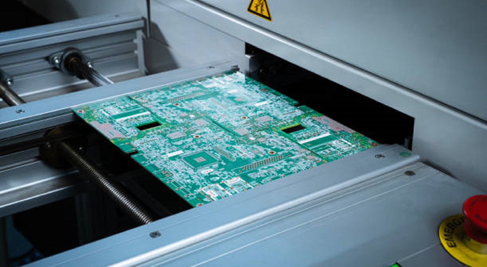
Equipment: Tools such as conveyors, reflow ovens, and pick-and-place machines can generate static electricity. Charge can be built up and discharged if equipment is not grounded.
Materials: PCBs, metalizers, and pack materials can accumulate electrostatic charges. Cleaning solutions and solder material are also possible sources.
Environment: Dry conditions and ventilation systems tend to increase static generation.
Lacking adequate precautions, these sources develop potentials that discharge onto sensitive electronics and damage them.
ESD Control Plan Components
Reducing ESD hazards requires creating a full ESD control plan. Such a plan must incorporate:
ESD Protected Spaces (EPA): Designate specific spaces with controlled environments, including humidity control and antistatic surfaces.
Correct Grounding Methods: Give grounding to everything and everybody to create safe routes for discharge of static electricity.
Handling Practices: Supply personnel with ESD safe supplies and techniques for handling delicate electronic components.
Packaging & Storage Solutions: Utilize conductive and antistatic materials to shield during storage and transport.
Routine Testing and Validations: Regularly check and audit to ensure compliance and ongoing effectiveness of ESD controls.
Installation of ESD Protected Areas
Implement EPAs in your plant:
Warning Signs: Use clear markings to identify sensitive areas and warn personnel of ESD risks.
Antistatic Infrastructure: Install EPA areas with floors and workstations of dissipative or conductive materials with appropriate grounding points.
Humidity Control: Maintain a relative humidity level of 40-60% to minimize the opportunity for static electricity buildup. Utilize ionizers where needed for charge neutralization.
Personnel Grounding: Use antistatic apparel, coats, and smocks, and conductive shoes with grounding straps for all operators.
Equipment and Personnel Grounding
Grounding efficiently is a core pillar of ESD protection:
Equipment Grounding: Implement single-point machine grounding and verify continuity. Earth ground metal chassis and do not use painted surfaces because they are insulators to charges.
Personnel Grounding: Implement wrist straps and conductive shoes that are verified daily for the correct resistance, maintaining the grounding resistance at 0.1 to 1M ohm.
Proper grounding reduces the likelihood of ESD events by providing controlled paths for static charges to dissipate safely.
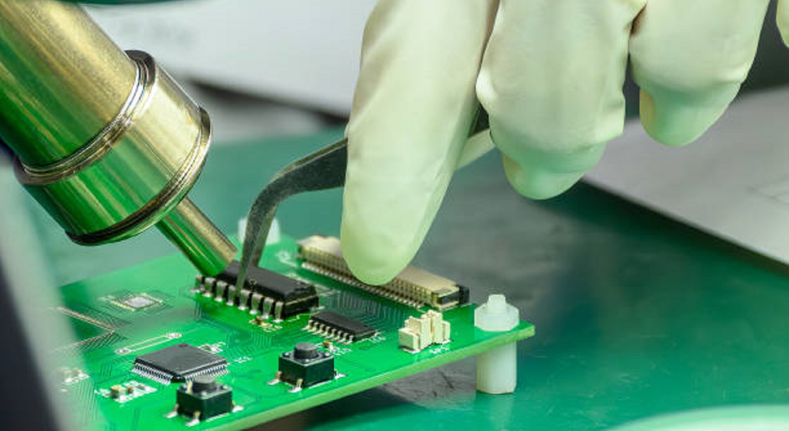
ESD Safe Handling Procedures
Adopt stringent procedures while handling PCBs and components:
Grounding: Use a grounded wrist strap at all times before handling ESD-sensitive devices. Ensure grounding equipment is under check and properly maintained at regular intervals.
Handling Techniques: Stay away from direct contact with the terminals or pins of the components. Handle devices by the edges and use vacuum pickup tools.
Antistatic Materials: Use only approved packaging and containers that eliminate the use of regular plastics or cardboards for ESD-sensitive devices.
ESD Safe Packaging and Storage
Components are shipped and stored in static-controlled packaging:
Material Selection: Choose conductive or static-dissipative packaging materials for effective protection.
Package Forms: Use conductive trays, tubes, and bags. Metalized shielded bags offer added protection for sensitive components.
Labeling: Label storage with ESD caution and sensitivity levels in clear terms to ensure proper handling by everyone.
Testing and Validation Methods
Reliable testing and validation methods are needed to ascertain ESD control effectiveness:
Compliance Verification: Utilize voltage probes to observe electrical potentials on conductors and use resistance measurements to ensure proper grounding.
Process Validation: Conduct simulated ESD events and observe handling practice to ensure protocols.
Audit Trails: Maintain regular inspections and corrective actions to treat any departures from specified standards and protocols.
A successful ESD control strategy for SMT assembly is needed that balances environmental, equipment, personnel, and procedural factors. We have included these best practices at PCBX to bestow our electronic assemblies with the greatest degree of quality and reliability. Continuing relentless vigilance and following ESD best practices, we virtually remove risks associated with ESD, delivering solid and dependable PCB manufacturing outcomes. This comprehensive approach not only protects electronic assemblies from harm but also enhances overall production efficiency and reliability.
Hot Tags:

Contact us

If you can't find what you're looking for, please contact us.
Article
ESD standards like ANSI/ESD S20.20 protect electronics from electrostatic damage, ensuring product reliability and reducing risks in manufacturing.
 2025/01/07
SMT assembly streamlines electronics manufacturing with compact, reliable designs using precise equipment, meeting high-density demands and international standards.
2024/10/29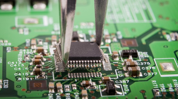
Still, SMT can further feature defects such as solder bridging, cold solder joints, tombstoning, and solder balling. Grasping the very common faults and their solutions is the key toward effective PCB assembly and reducing SMT errors—very much in line with the trend toward PCB miniaturization and higher component density.
2024/07/29