- Products & Capabilities

- About
- Resources
How to Solder BGA Components?


BGAs offer high-density interconnects and compact design, crucial for advanced electronics, but hidden solder joints complicate assembly, requiring precise methodologies.
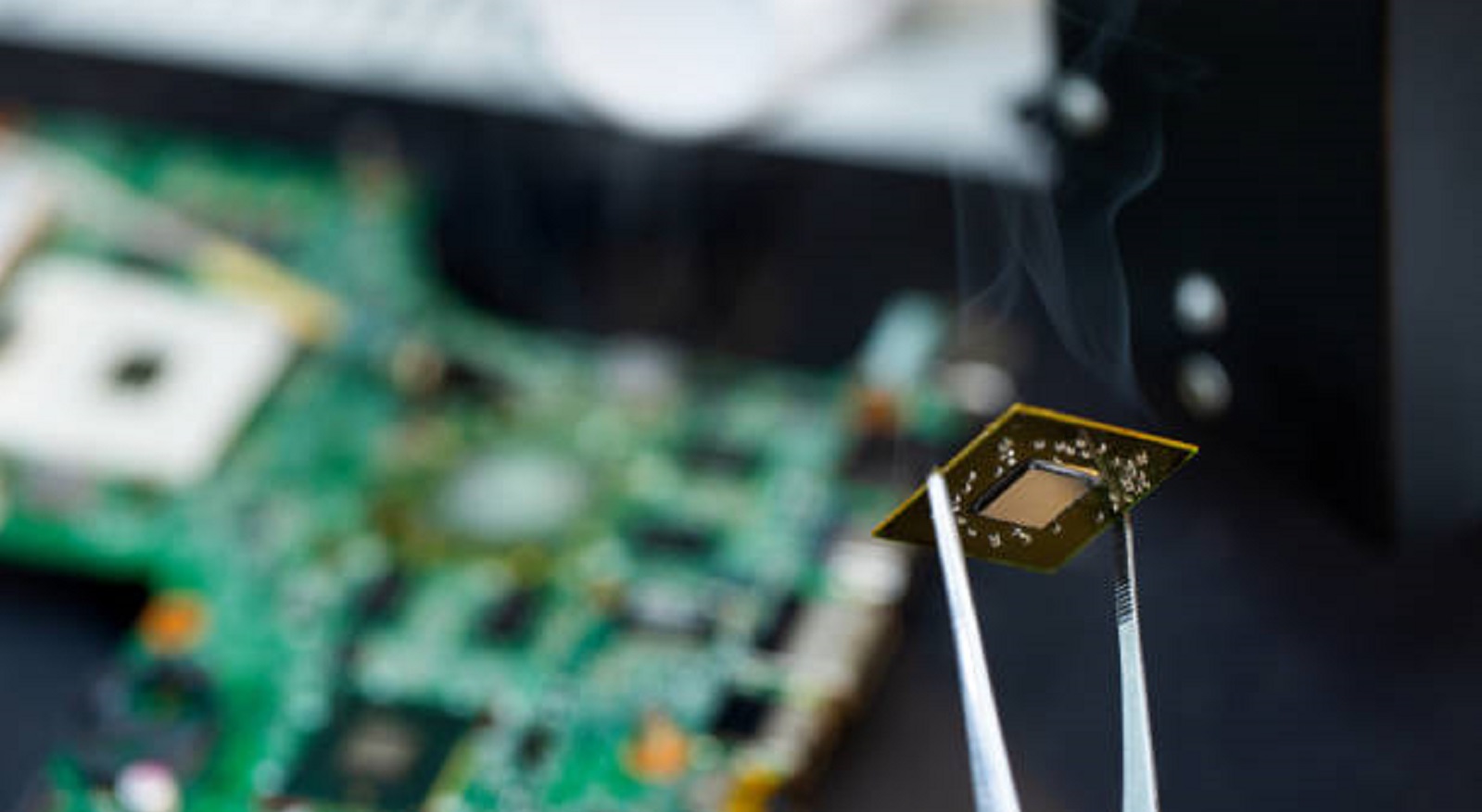
Ball Grid Array (BGA) devices are a backbone of modern electronics, as they possess tremendous high-density interconnect capabilities, with their miniature size making them an indispensable part of the sector. BGAs play an important role in complex designs, as they cater to advanced microprocessors, as well as sophisticated chipsets. BGAs, although an important part of modern electronics, possess certain complexities, mainly due to the invisible leads/solder joints on these devices.
BGA Packaging Technology Overview
In a BGA package, there is an array of balls below the surface. These balls make direct contact with a PCB's surface. A BGA package exhibits key features that can be listed below:
High-Density Interconnections: It is possible to package very large ICs containing well over a thousand pads on a BGA.
Compact Design: The grid array package has a compact design and can be mounted easily even in space-constrained designs.
Improved Electrical Performance: The shorter paths mean that there is less inductance, which enhances high-speed performance capabilities
Although the optimal design of BGAs provides a number of benefits, their assembly becomes a complex job owing to the concealed solder joints.
Advantages of Ball Grid Array Packaging
Some of the benefits that Ball Grid Arrays have over conventional leaded packages are:
Compactness: They have a smaller footprint which maximizes board space with reduced weight and minimal height of devices; these are ideal for miniaturized electronic devices.
Vulnerability: BGAs have strong solder joints that are highly resistant to damage rather than vulnerable leads.
Manufacturing Efficiency: With direct surface mount assembly, there are simplified processes for manufacturing, which facilitates faster and more precise production.
Improved Thermal Performance: This optimizes thermal distribution, reducing hotspots and increasing component lifespan.
In spite of these advantages, being a BGA interface, the solder joints are hidden, creating challenges to be addressed using unique methodologies and processes.
BGA Ball Soldering Challenges
Although BGAs allow miniaturization and performance improvements, they also pose a few difficulties:
Inspection Complexity: Because the solder joints are hidden under the BGA packages, the inspection cannot be performed in the conventional way and has to be carried out through techniques that are more complex in nature, like X-ray imaging
Reworking Difficulties: Reprocessing involves precise tools and techniques that have nothing to do with contact, such as hot air and infrared systems, and these can cause difficulties with some components.
Thermal Sensitivity: Incorrect thermal processes can give rise to problems in the board such as cracked joints, voids, or tombstoning.
Positional Accuracy: With a compact and grid-based component layout, it is important to be accurately positioned in its placement process because it is small in size.
To deal with such issues, sophisticated equipment, as well as expert approach, are needed right from the soldering process itself to the reworking stages.
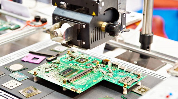
Essential BGA Soldering Processes
To be a BGA soldering expert, one has to become knowledgeable in several processes and pay close attention to:
PCB Land Patterns:
In designing the PCB pad formation, the land formation must be matched to the ball pitch of the BGA. The pads should be slightly larger than the balls, as recommended by the IPC for reliability purposes.
Solder Paste Application:
There is a requirement of laser-cut stencils and advanced printing technologies for paste deposition. To achieve reliability in BGA interconnecting joints, fine feature electroformed stencils and paste volume matching that of BGA balls have to be ensured.
Component Placement:
High-precision pick and place machines are essential for component positioning. Such machines use vision systems for precise component positioning. This is crucial for self-alignment in the reflow processes without adding stress to the solder balls.
Reflow Soldering:
Reflow soldering requires an even more precise temperature profile than conventional through-hole reflow soldiering. The critical phases of reflow soldering include preheating, soaking, and controlled cooling to create a consistent solder joint.
Solder Joint Inspection:
Inspection employs a technique that combines X-ray imaging with acoustic microscopy to identify any possible defects such as voids or misalignment that cannot be seen by the naked eye.
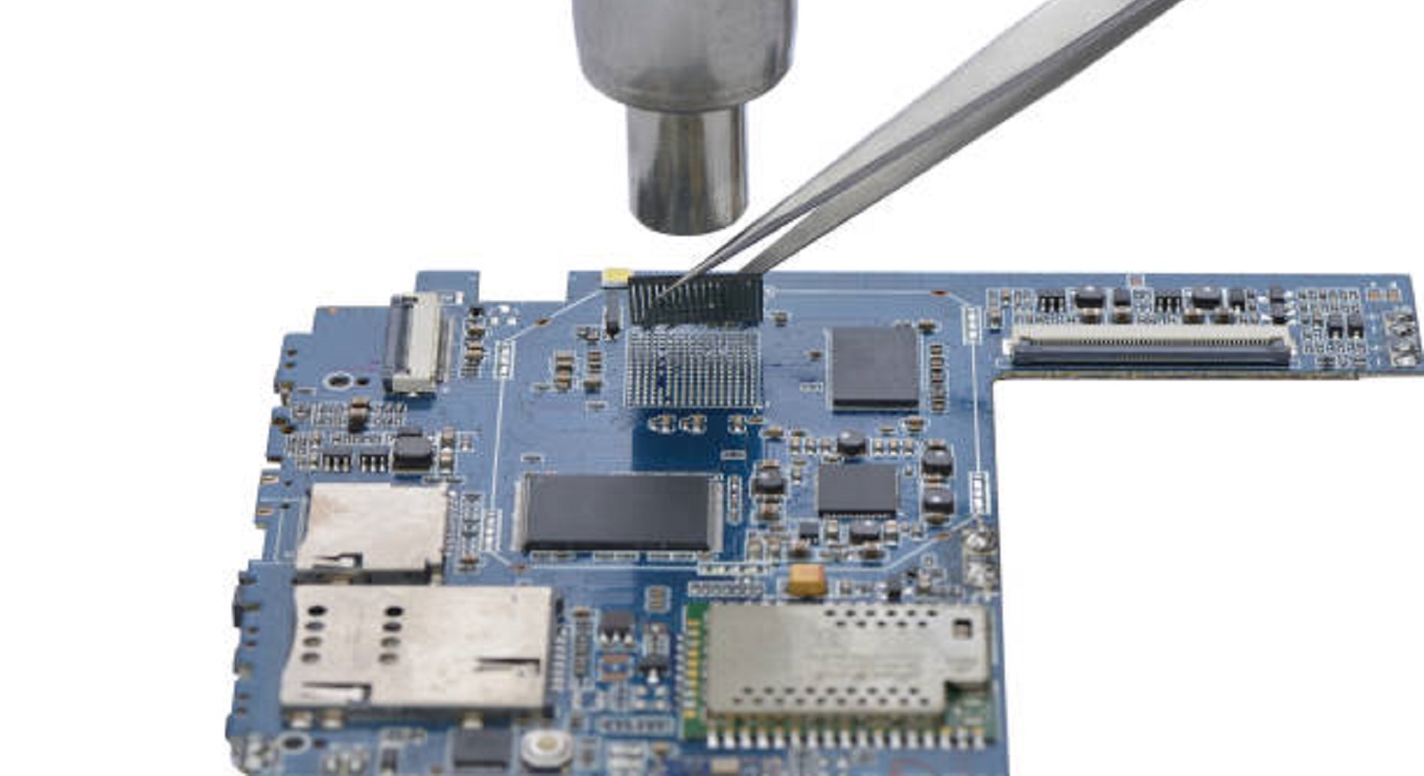
BGA Rework Strategies
Reworking ball grid array components involves precision and the necessary tools:
Preparation: Assessing the first assembly process for potential problem causes is an important step.
Removal: The uniform heating of the component using infrared or hot air guns helps in the removal of the component with minimal damage to the PCB or pads.
Site Redressing: Thorough cleaning of the pads on the PCBs and the reapplication of flux to these pads is required before the reinstallation or replacement of parts.
Reballing: Solder balls are added to a component using precise stenciling to form new contacts.
Replacement and Reflow: When the component is realigned and reflowed to form a fresh connection, it needs to follow a thermal profile.
BGA rework requires an understanding and application of process control and the use of tools with capabilities suitable for rework work.
The soldering of BGA components is a complex procedure that is achievable through the use of various technologies. It is important to note that the invisible solder interconnections in BGAs provide incredible performance if their complex requirements are carefully addressed. While the challenges posed by the potential of BGA components cannot be completely avoided in the entire lifetime of the product, appropriate use of equipment as well as methodological procedure can ensure that the performance requirements of the BGA components are not hampered.
Hot Tags:

Contact us

If you can't find what you're looking for, please contact us.
Article
BGA reballing restores functionality to failed solder joints using precise tools and methods, crucial for compact devices facing thermal, physical, or environmental stress.
 2025/04/29
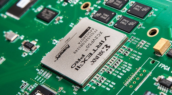
Ball Grid Array (BGA) components, such as PBGA, CBGA, CCGA, TBGA, and CSP, provide high I/O density, improved reliability, and high-quality electrical and thermal performance. Quality assembly and functionality are assured since advanced soldering and inspection methods are required, like AXI and AOI. Proper storage and handling shall guarantee the performance of the devices.
2024/07/26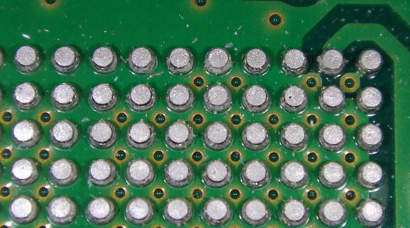
In the late 1980s, when electronics began to shrink, BGA packaging was developed to integrate more connections within a given area. Today, BGA is widely used with high-connection chips—processors being a good example. BGA uses solder balls at the bottom of the chip to connect it to the circuit board. It provides high density along with good heat dissipation and fast signal transmission, one of the main reasons it is ideal for modern electronics. However, it requires precise techniques of soldering in BGA manufacturing.
2024/07/24