- Products & Capabilities

- About
- Resources
PCB Backdrilling Process: Improve Signal Integrity in High-Speed PCB Design


Learn the PCB backdrilling process, how it removes via stubs, improves signal integrity, and enhances high-speed PCB performance.
The high-speed and high-frequency electronic systems have evolved at a very high rate thus necessitating the preservation of signal integrity in printed circuit boards (PCBs). Via stubs (unutilized plated through-holes) that may compromise signal quality is one of the most difficult issues in multilayer PCB design. To fix this problem, the PCB backdrilling process (also called controlled depth drilling (CDD)) is a common procedure that excises these undesirable conductive parts.
What is PCB Backdrilling?
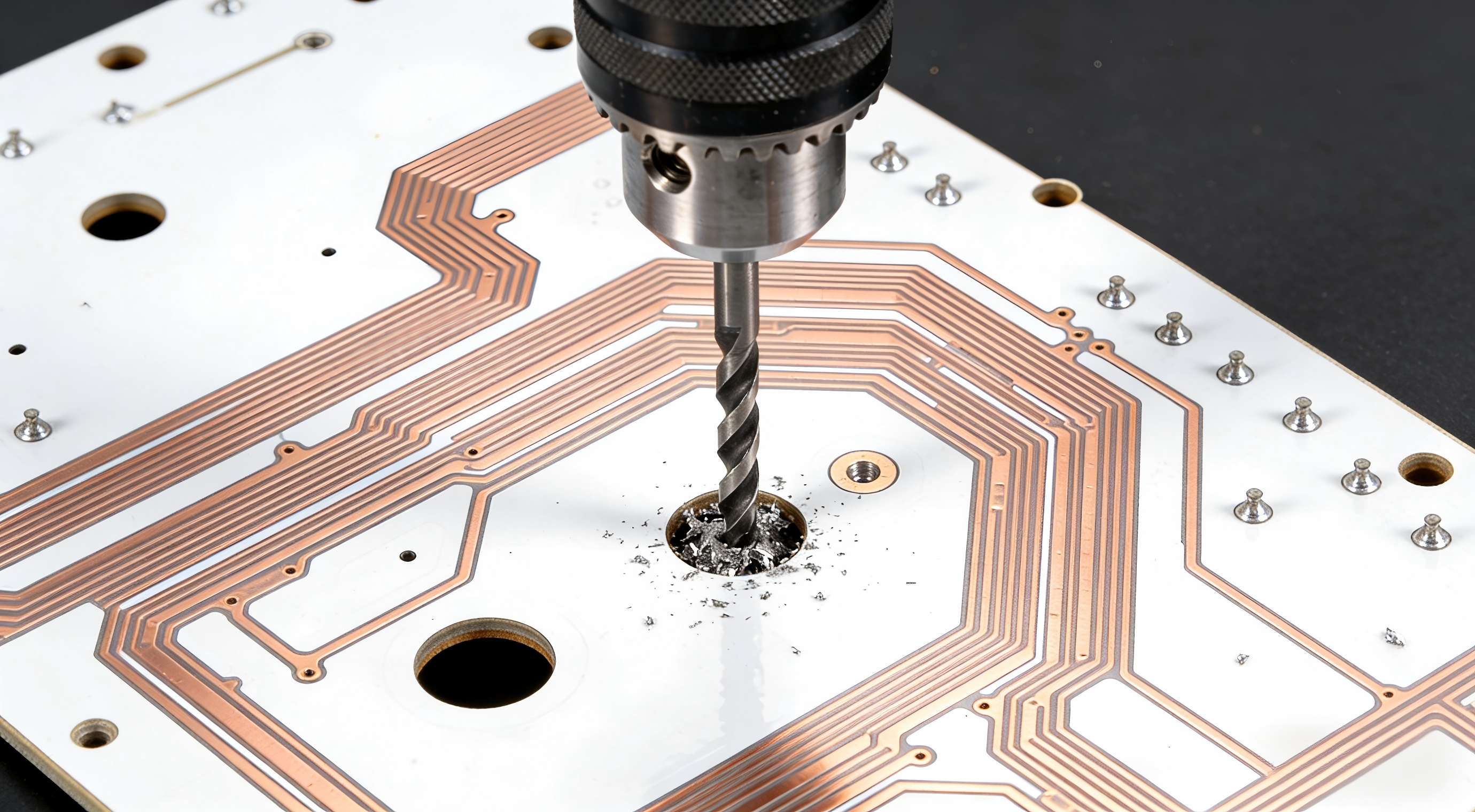
PCB backdrilling is a secondary drilling method that is applied to the unused copper part (via stub) of a plated through-hole when the primary drilling and plating has been finished.
In most multilayer PCBs, vias are drilled through the whole board to provide interlayer connections. But in cases where only two particular layers are connected by the signal, the other part of the via that is not used turns out to be a stub. These stubs can serve as unwanted transmission lines causing signal reflections and distortion particularly at high frequencies.
Backdrilling eliminates this unwanted material by re-drilling the via on one side of the board to a controlled depth with a slightly larger drill bit.
Why Backdrilling is Necessary
Elimination of Via Stub Effects
Via stubs create impedance discontinuities and act as resonators at high frequencies, refracting signals and losing energy.
Improved Signal Integrity
Signal reflections and distortion are greatly minimized by keeping stub length (usually not more than 10 mil) short.
Lower Jitter and Bit Error Rate (BER)
Via stubs cause deterministic jitter, which is a disadvantage of timing accuracy. Elimination of stubs aids in minimizing jitter and contributes to the overall signal reliability.
Reduced EMI and Crosstalk
Shorter conductive paths lower the electromagnetic interference (EMI) as well as unwanted coupling among signals.
PCB Backdrilling Process Flow
After via plating, the backdrilling process is normally part of PCB fabrication. The primary processing stages are:
Via Formation and Plating
Standard through-hole drilling and copper plating is then used to create conductive vias in the PCB.
Target Vias Identification
Design engineers define the vias that should be backdrilled depending on signal paths and usage of layers. Long unused segments of a via are given a higher priority.
Controlled Depth Drilling
The via is re-drilled using a CNC drilling machine; the via may be re-drilled on the top or bottom side of the board:
The hole in the drill has a slight greater diameter than the initial one.
Control of the depth of drilling is done to eliminate the stub without compromise of the active layers.
Minimal protection is provided to signal layers.
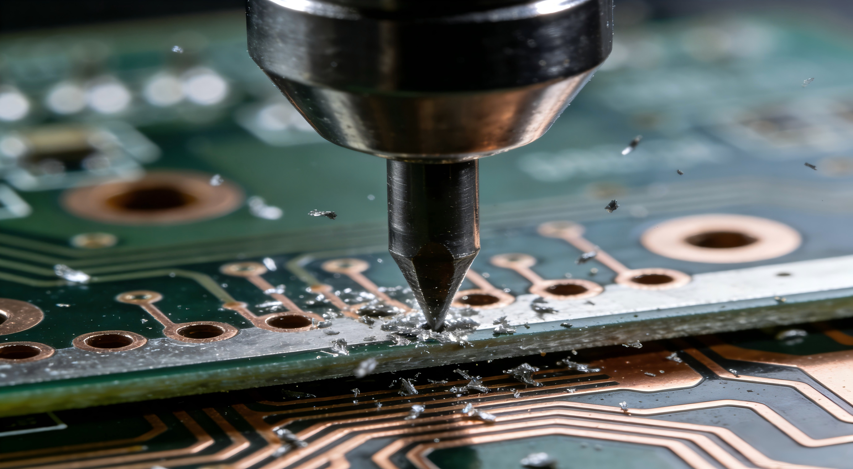
Quality Control and Inspection
After backdrilling:
Drilling depth is checked with x-ray or cross-section analysis.
Electrical tests make sure there is correct connection.
Key Design Considerations
Residual Stub Length
The backdrilling stub left behind should preferably be less than 10 mil in order to prevent signal degradation.
Drill Size Selection
The backdrill hole is usually bigger than the original via in order to remove all of the plated copper barrel.
Depth Control Accuracy
Accurate Z-axis movement is required. Excessive stub length can be left by under-drilling whereas signal layers can be damaged by over-drilling.
Clearance Requirements
Between the backdrilled hole and the surrounding copper features, there should be sufficient spacing to avoid short circuits or mechanical damage.
Advantages of Backdrilling
Enhances signal integrity as well in high-speed designs.
Minimizes signal reflection, attenuation and jitter.
Enhances impedance matching
Minimizes EMI and crosstalk
Enhances the reliability of the system.
Limitations and Challenges
High manufacturing cost as a result of extra drilling.
Increased complexity of processes that demand accurate equipment.
Designing density or intricate stackups.
Poor performance relative to more sophisticated methods such as blind or buried vias in others.
Alternatives to Backdrilling
Although backdrilling is a practical technique, via stub effects can be minimized by other techniques:
Blind and buried vias.
Microvias (laser-drilled vias)
Optimization of layer stack-up design.
Nevertheless, these options usually require more cost in fabrication or increased design complexity, so backdrilling is a viable trade off in most cases.
Best Practices
Backdrill requirements should be defined on fabrication drawings.
Work hand in hand with PCB producers at an early design stage.
Simulate signal integrity and stub impact.
Always exercise good tolerances to drill depth and diameter.
Only important high-speed signal paths should be limited to backdrilling.
Modern high-speed PCB design requires PCB backdrilling, which allows engineers to efficiently remove via stubs and increase signal integrity. Backdrilling can greatly enhance electrical workload with minimal modification of the structure, by simply keeping the depth of drilling small and the design parameters optimal.
It adds more manufacturing processes but the advantages in high-frequency applications are usually greater than the expenses. Backdrilling can be a good and cost-efficient method of getting high-performance PCB designs when done correctly. In more sophisticated PCB manufacturing and design solutions, PCBX provides full assistance to enable engineers to adopt the methods like backdrilling that are accurate and efficient.
Hot Tags:

Contact us

If you can't find what you're looking for, please contact us.
Article
PTH soldering provides strong connections by threading component leads through PCB holes, requiring meticulous preparation and quality checks for lasting results.
 2025/04/24
Understanding and correctly specifying PCB drill sizes ensure board functionality and manufacturability. Drill sizes affect electrical connections, stability, and signal integrity in PCB design and assembly.
2024/10/09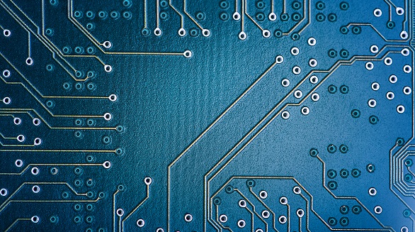
Annular rings are crucial for reliable PCB electrical connections. Proper sizing, understanding issues like tangency and breakout, and best practices ensure optimal performance and reliability in electronic circuits.
2024/09/18