- Products & Capabilities

- About
- Resources
Printed Circuit Board Failure Analysis


PCB failure analysis ensures reliable electronic devices by diagnosing defects, addressing manufacturing challenges, and optimizing design for improved performance.
Printed Circuit Boards (PCBs) are fundamental components of modern electronic devices, the building blocks for everything from the ordinary consumer electronics of the day-to-day gadgets and toys to complicated machinery like radar detectors and high-performance computing systems. Since the underlying structure that joins and sustains electronic components, PCBs must be strong and efficient. Malfunction in any section of a PCB can result in critical device failures or full system breakdowns. In this article, we examine the steps and issues involved in PCB failure analysis with the purpose of highlighting strategies that ensure quality assurance and optimized functionality.
Understanding the Critical Role of PCBs
PCBs are made up of intricate assemblies that integrate components such as capacitors, resistors, fuses, and diodes to enable electronic functions. They can perform single tasks or aid multiple functions and are available in three dominant forms: multilayer, double-sided, and single-sided configurations. While consumer demands increasingly require smaller and more advanced devices, design engineers face the challenge of creating smaller, advanced, and faster PCs. These boards must not only be economical but also meet high standards of quality. This atmosphere makes PCB failure analysis a necessity, providing data to enable improved design and manufacturing techniques.
The Need for PCB Failure Analysis
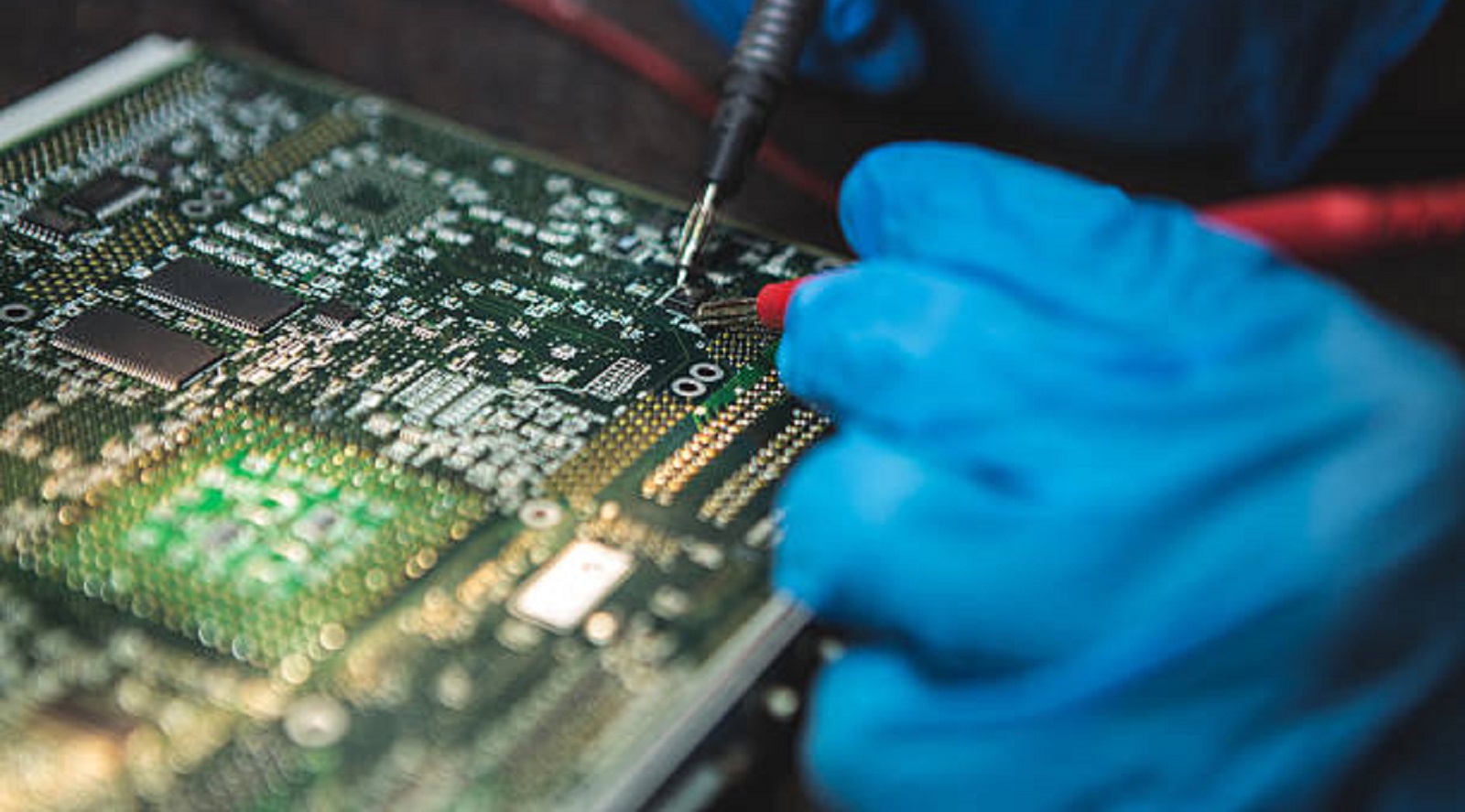
That there should be peak performance in PCBs within total electronic systems necessitates vigorous surveillance and comprehensive testing of all components. When failure occurs, PCBX engineers employ different techniques and tools to effectively diagnose the faults. Identification of the underlying causes of the failure is crucial so that actions can be initiated to prevent it that enhance product reliability and extend its life. Such analysis is particularly critical for high-risk applications like medical implants and space satellites, where PCB faults would mean catastrophic consequences.
Manufacturing and Failure Analysis Challenges
The modern PCB manufacturing environment presents several challenges that complicate failure analysis:
Requirements for Recycling: Environmental regulations for recycling dictate environmentally sound means of PCB manufacturing, impacting processes and materials.
Increased Circuit Density: Miniaturation technologies lead to denser circuit layout, exposing it to risk for accuracy and precision in manufacturing.
Precision Tuning: Maintaining PCBs within some electrical and performance specifications is necessary to minimize the risks of failure.
Lead-Free Soldering: Exceeding greater temperature requirements for lead-free components. Material Safety: Handling hazardous materials involves consideration to long-term reliability and the environment's impact.
Technological Evolution: More rapid progression of manufacturing technologies introduces new variables to production and test processes.
Root Cause Analysis: A Cornerstone of PCB Health
Root cause analysis is also one of the strong supports of effective PCB failure analysis. At PCBX, it is a structured process of failure mechanism analysis and corrective action. Through quantitative analysis, design teams receive valuable information that helps their products improve, correcting faults in initial designs undetected earlier. This feedback loop coexists with the overall objective of the industry to achieve zero-defect production, giving products high reliability.
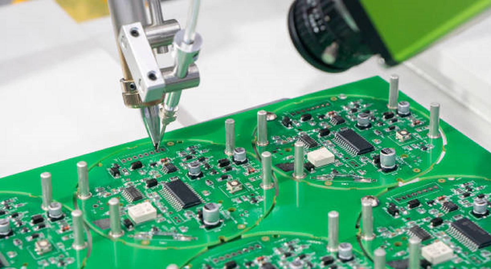
Types of Failure Analysis Tests
In a bid to identify and prevent defects in PCBs, PCBX employs various tests that are used to identify specific defects:
Solderability Testing: The test assesses the resistance of solder joints to various environments. It is important to ensure that the surface of the PCBs and the components is strong enough to establish solid solder joints and affect long-term product reliability.
Micro-sectioning Analysis (Metallographic Preparation): This process is utilized for inspection of various types of defects like shorts, opens, component defects, and raw material evaluation. Through a specified two-dimensional cut of the PCB, analysts are able to carefully inspect and solve specified vulnerabilities.
Optical Microscopy and Scanning Electron Microscopy (SEM): Optical microscopy remains the most popular method of fault identification of assembly and soldering quickly and effectively. SEM supplements this with in-depth analysis at a maximum of 120,000X magnifications such that even minor faults in integrated circuits can be analyzed.
PCB Contamination Testing: Contamination can lead to corrosion and degradation. The use of ionic contamination testing guarantees proper cleaning and manufacturing methods are employed to prevent undesirable effects on PCB integrity.
X-ray Inspection: X-ray technology provides a non-destructive method for examination of solder joints and internal parts beyond human vision. It allows technicians to detect defects without altering the PCB's pre-test condition, and this is of great help in failure analysis.
Overcoming Common PCB Manufacturing Challenges
PCB manufacturing complexity offers several potential defects. Analysts have to deal with factors such as:
Lead-Free Assembly Process: Soldering onto lead-free assemblies requires precise temperature control and various material selection.
High-Speed PCBs: The electrical performance of high-speed designs must be carefully planned to avoid signal degradation and interference.
Conductive Anodic Filament (CAF): Effective control of environmental and manufacturing conditions must be exercised to avoid CAF growth, leading to failure of the PCB.
Plated-Through Hole (PTH) Cracking: The mechanical integrity of plated-through holes must be maintained for the electrical continuity.
Surface Finishes Selection: Right selection of surface finishes must be made to provide consistent and reliable performance in a broad spectrum of operating conditions.
As the electronics industry continues to evolve, the need for effective and reliable PCBs becomes increasingly critical. At PCBX, we go the extra mile to ensure thorough design and fault-resistant failure analysis to prevent flaws and enhance product quality. By employing cutting-edge techniques and professional strategies, we strive to surpass stringent standards and render our products durable enough to face the challenge of modern technology. With relentless commitment to quality and precision, PCBX is committed to delivering reliable electronic solutions that shape the future.
Hot Tags:

Contact us

If you can't find what you're looking for, please contact us.
Article
PCBs are essential but prone to faults. Diagnosis and repair using tools like multimeters and X-rays prevent costly repairs, ensure reliability, and improve quality.
 2024/11/26
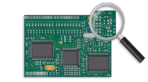
Routine inspections and proper maintenance of capacitors and resistors in PCBs reduce failures, prolong device lifespan, and lower maintenance costs.
2024/11/04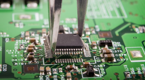
Still, SMT can further feature defects such as solder bridging, cold solder joints, tombstoning, and solder balling. Grasping the very common faults and their solutions is the key toward effective PCB assembly and reducing SMT errors—very much in line with the trend toward PCB miniaturization and higher component density.
2024/07/29