
- Products & Capabilities

- About
- Resources
Process Optimization and Quality Control for Multilayer PCB Lamination


Learn multilayer PCB lamination process optimization, key strategies for reducing voids, warpage and improving inter‑layer reliability for high‑performance circuit boards.
Multilayer PCBs are the indispensable core carrier of modern high-density electronic devices, widely deployed in 5G communication terminals, precision medical equipment, industrial automation systems, and aerospace electronic modules. As the key forming procedure that determines the overall structural integrity and electrical performance of multilayer boards, the lamination process bonds patterned inner core layers, resin-impregnated prepreg dielectrics, and outer copper foils into a unified compact structure through accurate thermal and pressure cycling. Improper parameter settings and unreasonable process control in traditional lamination production easily induce common defects including interlayer delamination, board warpage, micro voids, and inconsistent impedance values. These flaws not only reduce production yield and increase manufacturing costs but also seriously undermine signal integrity and long-term operational reliability of electronic equipment. Therefore, scientific and systematic optimization of the multilayer PCB lamination process is essential to stabilize product quality and meet strict IPC industrial manufacturing standards.
Basic Overview of Multilayer PCB Lamination
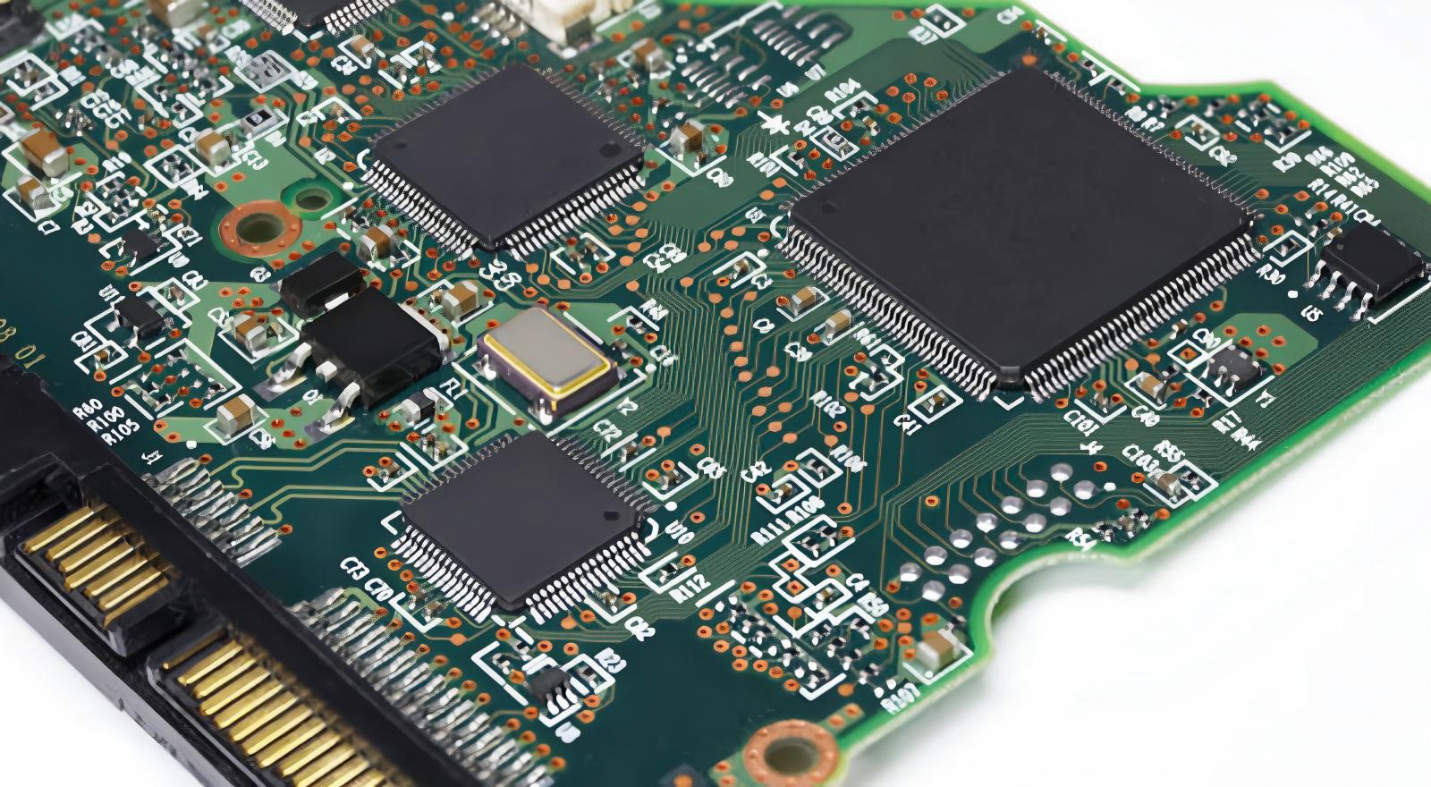
The multilayer PCB lamination process is based on the thermosetting cross-linking reaction of prepreg resin, featuring high-precision layer matching and thermocompression forming. The complete standardized workflow covers inner layer pretreatment, symmetrical stack-up assembly, precision layer alignment, vacuum hot pressing, constant-pressure cooling and systematic post-lamination inspection. After inner circuit patterning and etching, copper surfaces undergo professional roughening and browning treatment to form a uniform micro-texture, which effectively enhances the interfacial adhesion between copper foil and resin. All layers are stacked in a standardized symmetrical sequence and fixed via positioning holes to prevent layer misalignment. In the vacuum hot press, elevated temperature melts the prepreg resin to fully fill tiny gaps between dense circuit traces and interlayer spaces, before complete curing forms stable insulating dielectric layers. Every subtle change in process parameters will directly affect the dimensional accuracy, flatness and interlayer bonding strength of finished PCBs.
Necessity of Lamination Process Optimization
Most traditional PCB factories rely on empirical fixed parameters for lamination production, which cannot adapt to the manufacturing requirements of high-layer-count, high-frequency and high-density HDI PCBs. Unoptimized processes bring multiple quality risks that affect subsequent production and terminal application. Severe board warpage causes deviation in drilling and component mounting, leading to assembly failure; tiny interlayer voids reduce thermal conductivity and trigger high-frequency signal attenuation; insufficient resin filling results in weak interlayer bonding and delamination failure under long-term thermal cycling; uneven dielectric thickness causes severe impedance deviation, failing the 50±5 ohm impedance tolerance standard required for 5G and RF high-speed circuits. In contrast, refined process optimization can eliminate common lamination defects, improve manufacturing consistency, and greatly reduce product scrap rate and comprehensive production costs.
Core Optimization Strategies for Lamination Process
Scientific Material Selection and Compatibility Matching
Material compatibility is the fundamental premise of high-quality lamination molding. Manufacturers need to select matched core substrates, prepreg dielectrics and copper foils according to product application scenarios and performance indicators. Conventional FR-4 substrates with stable comprehensive performance are suitable for ordinary consumer electronic products, while low-Dk and low-loss dielectric materials are selected for high-speed and high-frequency communication products to reduce signal transmission loss. The prepreg resin content is strictly controlled within 40% to 60% to balance resin fluidity and filling sufficiency during thermocompression. In addition, matching the coefficient of thermal expansion (CTE) of different materials avoids excessive internal thermal stress, and adopting uniform-thickness copper foil effectively prevents unexpected impedance fluctuations across the board surface.
Symmetrical and Precise Stack-Up Design
Asymmetric stack-up structure is the primary cause of lamination warpage and dimensional distortion. The optimized stack-up scheme strictly follows central symmetry principles, keeping balanced copper density, dielectric thickness and material distribution on both sides of the board centerline. For high-precision HDI multilayer boards, refined dielectric thickness planning is adopted to realize accurate impedance control within standard tolerance ranges. Meanwhile, multi-point positioning holes and mechanical riveting fixation are used for auxiliary layer alignment, which controls the layer offset error within 0.05 mm and fundamentally avoids open-circuit and short-circuit risks of fine-pitch circuit traces.
Dynamic Precision Parameter Control
Temperature, pressure, holding time and vacuum degree are the four core controllable parameters of the lamination process. The optimal industrial process window sets curing temperature at 180–200°C, forming pressure at 300–500 psi, and curing time ranging from 60 to 120 minutes, with dynamic adjustment according to board layer count and material glass transition temperature (Tg). Different from the rigid fixed parameters of traditional processes, segmented gradient control is applied: low-temperature slow preheating ensures uniform resin softening and wetting, mid-stage pressurization promotes full resin filling of micro gaps, and constant-temperature heat preservation guarantees complete resin cross-linking and curing. A high-vacuum working environment thoroughly removes trapped air and volatile substances between layers, drastically reducing micro-void defects.
Complete Post-Lamination Quality Control
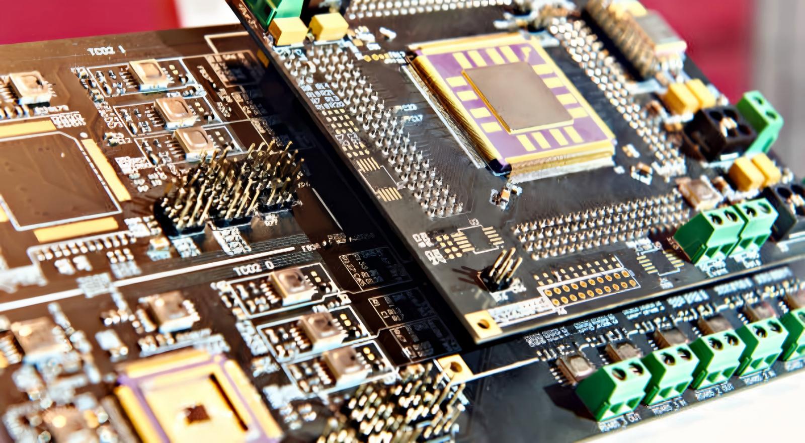
Sustainable process optimization must be supported by a complete quality inspection and feedback mechanism. After lamination, automated optical inspection (AOI) and X-ray detection are used to quickly identify layer deviation, resin starvation and micro bubble defects. Standard thermal stress tests compliant with IPC-TM-650 specifications verify interlayer bonding stability and thermal shock resistance. Regular cross-section sampling analysis eliminates hidden quality risks and provides data support for parameter iteration. For ultra-high-layer complex PCBs, segmented sequential lamination technology is adopted to disperse internal stress, further reduce board warpage, and improve overall structural stability.
Multilayer PCB lamination optimization is a systematic engineering improvement covering material matching, structural stack-up design, dynamic parameter tuning and full-process quality supervision. Comprehensive optimization can effectively reduce lamination defect rates, stabilize dielectric thickness and impedance performance, and significantly enhance the structural stability and environmental adaptability of multilayer PCBs, fully meeting the high-standard manufacturing needs of high-end electronic industries. For high-precision, high-reliability multilayer PCB customization and mass production, PCBX provides mature lamination process optimization solutions and strict full-link quality control systems, delivering consistent, high-performance PCB products for industrial control, communication, aerospace and other high-end scenarios.
Hot Tags:

Contact us

If you can't find what you're looking for, please contact us.
Article
3-layer PCBs offer a balance of cost and complexity with benefits like improved signal integrity, reduced EMI, and increased component density for varied applications.
 2025/01/22
PCBX offers fast, high-quality turn-key PCB prototype assembly services, including fabrication, component sourcing, and testing, all at competitive prices, to accelerate product development.
2024/08/14
Multilayer PCBs, essential for advanced electronics, offer compact size, lightweight, and high performance, making them ideal for various applications despite higher costs and complexity.
2024/08/06